

FUNDAMENTALS OF
COMPUTER
ORGANIZATION AND
ARCHITECTURE
Mostafa Abd-El-Barr
King Fahd University of Petroleum & Minerals (KFUPM)
Hesham El-Rewini
Southern Methodist University
A JOHN WILEY & SONS, INC PUBLICATION
FUNDAMENTALS OF
COMPUTER ORGANIZATION AND
ARCHITECTURE
WILEY SERIES ON PARALLEL AND DISTRIBUTED COMPUTING
SERIES EDITOR: Albert Y. Zomaya
Parallel & Distributed Simulation Systems / Richard Fujimoto
Surviving the Design of Microprocessor and Multimicroprocessor Systems:
Lessons Learned / Veljko Milutinovic
Mobile Processing in Distributed and Open Environments / Peter Sapaty
Introduction to Parallel Algorithms / C. Xavier and S.S. Iyengar
Solutions to Parallel and Distributed Computing Problems: Lessons from
Biological Sciences / Albert Y. Zomaya, Fikret Ercal, and Steph an Olariu (Editors)
New Parallel Algorithms for Direct Solution of Linear Equations /
C. Siva Ram Murthy, K.N. Balasubramanya Murthy, and Sriniva s Aluru
Practical PRAM Programming / Joerg Kell er, Christoph Kessler, and
Jesper Larsson Traeff
Computational Collective Intelligence / Tadeusz M. Szuba
Parallel & Distributed Computing: A Survey of Model s, Paradigms, and
Approaches / Claudia Leopold
Fundamentals of Distributed Object Systems: A CORBA Perspective /
Zahir Tari and Omran Bukhres
Pipelined Processor Farms: Structured Design for Embedded Parallel
Systems / Martin Fleury and Andrew Downton
Handbook of Wireless Networks and Mobile Computing / Ivan Stoj menoviic
(Editor)
Internet-Based Workflow Management: Toward a Semantic Web /
Dan C. Marinescu
Parallel Computing on Heterogeneous Networks / Alexey L. Lastovetsky
Tools and Environments for Parallel and Distributed Computing Tools /
Salim Hariri and Manish Parashar
Distributed Computing: Fundamentals, Simulations and Advanced Topics,
Second Edition / Hagit Attiya and Jennifer Welch
Smart Environments: Technology, Protocols and Applications /
Diane J. Cook and Sajal K. Das (Editors)
Fundamentals of Computer Organization and Architecture / M. Abd-El-Barr
and H. El-Rewini

FUNDAMENTALS OF
COMPUTER
ORGANIZATION AND
ARCHITECTURE
Mostafa Abd-El-Barr
King Fahd University of Petroleum & Minerals (KFUPM)
Hesham El-Rewini
Southern Methodist University
A JOHN WILEY & SONS, INC PUBLICATION
This book is printed on acid-free paper.
1
Copyright # 2005 by John Wiley & Sons, Inc. All rights reserved.
Published by John Wiley & Sons, Inc., Hoboken, New Jersey.
Published simultaneously in Canada.
No part of this publication may be reproduced, stored in a retrieval system, or transmitted in any form or
by any means, electronic, mechanical, photocopying, recording, scanning, or otherwise, except as
permitted under Section 107 or 108 of the 1976 United States Copyright Act, without either the prior
written permission of the Publisher, or authorization through payment of the appropriate per-copy
fee to the Copyright Clearance Center, Inc., 222 Rosewood Drive, Danvers, MA 01923,
for permission should be addressed to the Permissions Department, John Wiley & Sons, Inc.,
111 River Street, Hoboken, NJ 07030; (201) 748-6011, fax (201) 748-6008.
Limit of Liability/Disclaimer of Warranty: While the publisher and author have used their best efforts
in preparing this book, they make no representations or warranties with respect to the accuracy or
completeness of the contents of this book and specifically disclaim any implied warranties of
merchantability or fitness for a particular purpose. No warranty may be created or extended by sales
representatives or written sales materials. The advice and strategies contained herein may not be
suitable for your situation. You should consult with a professional where appropriate. Neither the
publisher nor author shall be liable for any loss of profit or any other commercial damages, including
but not limited to special, incidental, consequential, or other damages.
For general information on our other products and services please contact our Customer Care Department
within the U.S. at 877-762-2974, outside the U.S. at 317-572-3993 or fax 317-572-4002.
Wiley also publishes its books in a variety of electronic formats. Some content that appears in print,
however, may not be available in electronic format.
Library of Congress Cataloging-in-Publication Data:
Abd-El-Barr, Mostafa.
Fundamentals of computer organization and architecture / Mostafa Abd-El-Barr, Hesham El-Rewini
p. cm. — (Wiley series on parallel and distributed computing)
Includes bibliographical references and index.
ISBN 0-471-46741-3 (cloth volume 1) — ISBN 0-471-46740-5 (cloth volume 2)
1. Computer architecture. 2. Parallel processing (Electronic computers) I. Abd-El-Barr, Mostafa, 1950–
II. Title. III. Series.
QA76.9.A73E47 2004
004.2
0
2—dc22
2004014372
Printed in the United States of America
10987654321
978-750-8400, fax 978-646-8600, or on the web at www.copyright.com. Requests to the Publisher
To my family members (Ebtesam, Muhammad, Abd-El-Rahman, Ibrahim, and Mai)
for their support and love
—Mostafa Abd-El-Barr
To my students, for a better tomorrow
—Hesham El-Rewini

&
CONTENTS
Preface xi
1. Introduction to Computer Systems 1
1.1. Historical Background 2
1.2. Architectural Development and Styles 4
1.3. Technological Development 5
1.4. Performance Measures 6
1.5. Summary 11
Exercises 12
References and Further Reading 14
2. Instruction Set Architecture and Design 15
2.1. Memory Locations and Operations 15
2.2. Addressing Modes 18
2.3. Instruction Types 26
2.4. Programming Examples 31
2.5. Summary 33
Exercises 34
References and Further Reading 35
3. Assembly Language Programming 37
3.1. A Simple Machine 38
3.2. Instructions Mnemonics and Syntax 40
3.3. Assembler Directives and Commands 43
3.4. Assembly and Execution of Programs 44
3.5. Example: The X86 Family 47
3.6. Summary 55
Exercises 56
References and Further Reading 57
4. Computer Arithmetic 59
4.1. Number Systems 59
4.2. Integer Arithmetic 63
vii
4.3 Floating-Point Arithmetic 74
4.4 Summary 79
Exercises 79
References and Further Reading 81
5. Processing Unit Design 83
5.1. CPU Basics 83
5.2. Register Set 85
5.3. Datapath 89
5.4. CPU Instruction Cycle 91
5.5. Control Unit 95
5.6. Summary 104
Exercises 104
References 106
6. Memory System Design I 107
6.1. Basic Concepts 107
6.2. Cache Memory 109
6.3. Summary 130
Exercises 131
References and Further Reading 133
7. Memory System Design II 135
7.1. Main Memory 135
7.2. Virtual Memory 142
7.3. Read-Only Memory 156
7.4. Summary 158
Exercises 158
References and Further Reading 160
8. Input–Output Design and Organization 161
8.1. Basic Concepts 162
8.2. Programmed I/O 164
8.3. Interrupt-Driven I/O 167
8.4. Direct Memory Access (DMA) 175
8.5. Buses 177
8.6. Input –Output Interfaces 181
8.7. Summary 182
Exercises 183
References and Further Reading 183
viii CONTENTS
9 Pipelining Design Techniques 185
9.1. General Concepts 185
9.2. Instruction Pipeline 187
9.3. Example Pipeline Processors 201
9.4. Instruction-Level Parallelism 207
9.5. Arithmetic Pipeline 209
9.6. Summary 213
Exercises 213
References and Further Reading 215
10 Reduced Instruction Set Computers (RISCs) 215
10.1. RISC/CISC Evolution Cycle 217
10.2. RISCs Design Principles 218
10.3. Overlapped Register Windows 220
10.4. RISCs Versus CISCs 221
10.5. Pioneer (University) RISC Machines 223
10.6. Example of Advanced RISC Machines 227
10.7. Summary 232
Exercises 233
References and Further Reading 233
11 Introduction to Multiprocessors 235
11.1. Introduction 235
11.2. Classification of Computer Architectures 236
11.3. SIMD Schemes 244
11.4. MIMD Schemes 246
11.5. Interconnection Networks 252
11.6. Analysis and Performance Metrics 254
11.7. Summary 254
Exercises 255
References and Further Reading 256
Index 259
CONTENTS ix

&
PREFACE
This book is intended for students in computer engineering, computer science,
and electrical engineering. The mater ial cover ed in the book is suitable for a one-
semester course on “Computer Organization & Assembly Language” and a one-
semester course on “Computer Architecture.” The book assumes that students
studying computer organization and/or computer architecture must have had
exposure to a basic course on digital logic design and an introductory course on
high-level computer language.
This book reflects the authors’ experience in teaching courses on computer organ-
ization and computer architecture for more than fifteen years. Most of the material
used in the book has been used in our undergraduate classes. The coverage in the
book takes basically two viewpoints of computers. The first is the programmer’s
viewpoint and the second is the overall structure and function of a computer. The
first viewpoint covers what is normally taught in a junior level course on Computer
Organization and Assembly Language while the second viewpoint covers what is
normally taught in a senior level course on Computer Architecture. In what follows,
we provide a chapter-by-chapter review of the material covered in the book. In doing
so, we aim at providing course instructors, students, and practicing engineers/scien-
tists with enough information that can help them select the appropriate chapter or
sequences of chapters to cover/review.
Chapter 1 sets the stage for the material presented in the remaining chapters. Our
coverage in this chapter starts with a brief historical review of the development of
computer systems. The objective is to understand the factors affecting computing
as we know it today and hopefully to forecast the future of computation. We also
introduce the general issues related to general-purpose and special-purpose
machines. Computer systems can be defined through their interfaces at a number
of levels of abstraction, each providing functional support to its predecessor. The
interface between the application programs and high-level language is referred to
as Language Architecture. The Instruction Set Architecture defines the interface
between the basic machine instruction set and the Runtime and I/O Control.A
different definition of computer architecture is built on four basic viewpoints.
These are the structure, the organization, the implementation, and the performance.
The structure d efines the interconnection of various hardware components, the
organization defines the dynamic interplay and management of the various com-
ponents, the implementation defines the detailed design of hardware components,
and the performance specifies the behavior of the computer system. Architectural
xi
development and styles are covered in Chapter 1. We devote the last part of our cov-
erage in this chapter to a discussion on the different CPU performance measures
used.
The sequence consisting of Chapters 2 and 3 introduces the basic issues related to
instruction set architecture and assembly language programming. Chapter 2 covers
the basic principles involved in instruction set architecture and design. We start by
addressing the issue of storing and retrieving information into and from memory,
followed by a discussion on a number of different addressing modes. We also
explain instruction execution and sequencing in some detail. We show the appli-
cation of the presented addressing modes and instruction characteristics in writing
sample segment codes for performing a number of simple programming tasks.
Building on the material presented in Chapter 2, Chapter 3 considers the issues
related to assembly language program ming. We introduce a programmer’s view
of a hypothetical machine. The mnemonics and syntax used in representing the
different instructions for the machine model are then introduced. We follow that
with a discussion on the execution of assembly program s and an assembly language
example of the X86 Intel CISC family.
The sequence of chapters 4 and 5 covers the design and analysis of arithmetic cir-
cuits and the design of the Central Processing Unit (CPU). Chapter 4 introduces the
reader to the fundamental issues related to the arithmetic operations and circuits
used to support computation in computers. We first introduce issues such as number
representations, base conversion, and integer arithmetic. In particular, we introduce
a number of algorithms together with hardware schemes that are used in performing
integer addition, subtraction, multiplication, and division. As far as floating-point arith-
metic, we introduce issues such as floating-point representation, floating-point oper-
ations, and floating-point hardware schemes. Chapter 5 covers the main issues
related to the organization and design of the CPU. The primary function of the CPU
is to execute a set of instructions stored in the computer’s memory. A simple CPU con-
sists of a set of registers, Arithmetic Logic Unit (ALU), and Control Unit (CU). The
basic principles needed for the understanding of the instruction fetch-execution
cycle, and CPU register set design are first introduced. The use of these basic principles
in the design of real machines such as the 8086 and the MIPS are shown. A detailed
discussion on a typical CPU data path and control unit design is also provided.
Chapters 6 and 7 combined are dedicated to Memory System Design. A typical
memory hierarchy starts with a small, expensive, and relatively fast unit, called the
cache. The cache is followed in the hierarchy by a larger, less expensive, and rela-
tively slow main memory unit. Cache and main memory are built using solid-state
semiconductor material. They are followed in the hierarchy by a far larger, less
expensive, and much slower mag netic memories that consist typically of the
(hard) disk and the tape. We start our discussion in Cha pter 6 by analyzing the fac-
tors influencing the success of a memory hierarchy of a computer. The remaining
part of Chapter 6 is devoted to the design and analysis of cache memories. The
issues related to the design and analysis of the main and the virtual memory are
covered in Chapter 7. A brief coverage of the different read-only memory (ROM)
implementations is also provided in Chapter 7.
xii PREFACE
I/O plays a crucial role in any modern computer system. A clear understanding
and appreciation of the fundamentals of I/O operations, devices, and interfaces are
of great importance. The focus of Chapter 8 is a study on input – outpu t (I/O) design
and organization. We cover the basic issues related to programmed and Interrupt-
driven I/O. The interrupt architecture in real machines such as 8086 and
MC9328MX1/MXL AITC are explained. This is followed by a detailed discussion
on Direct Memory Access (DMA), busses (synchronous and asynchronous), and
arbitration schemes. Our coverage in Chapter 8 concludes with a discussion on
I/O interfaces.
There exists two basic techniques to increase the instruction execution rate of a
processor. These are: to increase the clock rate, thus decreasing the instruction
execution time, or alternatively to increase the number of instructions that can be
executed simultaneously. Pipelining and instruction-level parallelism are examples
of the latter technique. Pipelining is the focus of the discussion provided in Chapter
9. The idea is to have more than one instruction being processed by the processor at
the same time. This can be achieved by dividing the execution of an instruction
among a number of sub-units (stages), each performing part of the required oper-
ations, i.e., instruction fetch, instruction decode, operand fetch, instruction
execution, and store of results. Performance measures of a pipeline processor are
introduced. The main issues contributing to instruction pipeline hazards are dis-
cussed and some possible solutions are introduced. In addition, we present the con-
cept of arithmetic pipelining together with the problems involved in designing such
pipeline. Our coverage concludes with a review of two pipeline processors, i.e., the
ARM 1026EJ-S and the UltraSPARC-III.
Chapter 10 is dedicated to a study of Reduced Instruction Set Computers (RISCs).
These machines represent a noticeable shift in computer architecture paradigm. The
RISC paradigm emphasizes the enhancement of computer architectures with the
resources needed to make the execution of the most frequent and the most time-
consuming operations most efficient. RISC-based machines are characterized by
a number of common features, such as, simple and reduced instruction set, fixed
instruction format, one instruction per machine cycle, pipeline instruction fetch/exe-
cute units, ample number of general purpose registers (or alternatively optimized
compiler code generation), Load/Store memory operations, and hardwired control
unit design. Our coverage in this chapter starts with a discussion on the evolution
of RISC architectures and the studies that led to their introduction. Overlapped Reg-
ister Windows, an essential concept in the RISC development, is also discussed. We
show the application of the basic RISC principles in machines such as the Berkeley
RISC, the Stanford MIPS, the Compaq Alpha, and the SUN UltraSparc.
Having covered the essential issues in the design and analysis of uniprocessors
and pointing out the main limitations of a single stream machine, we provide an
introduction to the basic concepts related to multiprocessors in Chapter 11. Here
a number of processors (two or more) are connected in a manner that allows them
to share the simultaneous execution of a single task. The main advantage for
using multiprocessors is the creation of powerful com puters by connecting many
existing smaller ones. In addition, a multiprocessor consisting of a number of
PREFACE xiii
single uniprocessors is expected to be more cost effective than building a high-
performance single processor. We present a number of different topologies used
for interconnecting multiple processors, different classification schemes, and a
topology-based taxonomy for interconnection networ ks. Two memory-organization
schemes for MIMD (multiple instruction multiple data ) multiprocessors, i.e., Shared
Memory and Message Passing, are also introduced. Our coverage in this chapter
ends with a touch on the analysis and performance metrics for multiprocessors.
Interested readers are referred to more elaborate discussions on multiprocessors in
our book entitled Advanced Computer Architectures and Parallel Processing,
John Wiley and Sons, Inc., 2005.
From the above chapter-by-chapter review of the topics covered in the book, it
should be clear that the chapt ers of the book are, to a great extent, self-containe d
and inclusive. We believe that such an approach should help course instructors to
selectively choose the set of chapters suitable for the targeted curriculum. However,
our experience indicates that the group of chapters consi sting of Chapters 1 to 5 and
8 is typically suitable for a junior level course on Computer Organization and
Assembly Language for Computer Science, Computer Engineering, and Electrical
Engineering students. The group of chapters consisting of Chapters 1, 6, 7, 9–11
is typi cally suitable for a senior level course on Computer Architecture. Practicing
engineers and scientists will find it feasible to selectively consult the material cov-
ered in individual chapters and/or groups of chapters as indicated in the chapter-by-
chapter review. For example, to find more about memory system design, interested
readers may consult the sequence consisting of Chapters 6 and 7.
ACKNOWLEDGMENTS
We would like to express our thanks and appreciation to a number of people who
have helped in the preparati on of this book. Students in our Computer Organization
and Computer Architecture courses at the University of Saskatchewan (UofS),
SMU, KFUPM, and Kuwait University have used drafts of different chapters and
provided us with useful feedback and comments that led to the improvement of
the presentation of the material in the book; to them we are thankful. Our colleagues
Donald Evan, Fatih Kocan, Peter Seidel, Mitch Thornton, A. Naseer, Habib
Ammari, and Hakki Cankaya offered constructive comments and excellent sugges-
tions that led to noticeable improveme nt in the style and presentation of the book
material. We are indebted to the anonymous reviewers arranged by John Wiley
for their suggestions and corrections. Special thanks to Albert Y. Zoma ya, the
series editor and to Val Moliere, Kirsten Rohstedt, and Christine Punzo of John
Wiley for their help in making this book a reality. Of course, responsibility for
errors and inconsistencies rests with us. Finally, and most of all, we want to thank
our families for their patience and support during the writing of this book.
M
OSTAFA ABD-EL-BARR
HESHAM EL-REWINI
xiv PREFACE

&
CHAPTER 1
Introduction to Computer Systems
The technological advances witnessed in the computer industry are the result of a
long chain of immense and successful efforts made by two major forces. These
are the academia, represented by university research centers, and the industry,
represented by computer companies. It is, however, fair to say that the current tech-
nological advances in the computer industry owe their inception to university
research centers. In order to appreciate the current technol ogical advances in the
computer industry, one has to trace back through the history of computers and
their development. The objective of such historical review is to understa nd the
factors affecting computing as we know it today and hopefully to forecast the
future of computation. A great majority of the computers of our daily use are
known as general purpose machines. These are machines that are built with no
specific application in mind, but rather are capable of performing computation
needed by a diversity of applications. These machines are to be distinguished
from those built to serve (tailored to) specific applications. The latter are known
as special purpose machines. A brief historical background is given in Section 1.1.
Computer systems have conventional ly been defined through their interfaces at
a number of layered abstraction levels, each providing functional support to its pre-
decessor. Included among the levels are the application programs, the high-level
languages, and the set of machine instructions. Based on the interface between
different levels of the system, a number of computer architectures can be defined.
The interface between the application programs and a high-level language is
referred to as a language architecture. The instruction set architecture defines the
interface between the basic machine instruction set and the runtime and I/O control.
A different definition of computer architecture is built on four basic viewpoints.
These are the structure, the organization, the implementation, and the performance.
In this definition, the structure defines the interconnection of various hardware com-
ponents, the organization defines the dynamic interplay and management of the
various components, the implementation defines the detailed design of hardware
components, and the performance specifies the behavior of the computer system.
Architectural development and styles are covered in Section 1.2.
1
Fundamentals of Computer Organization and Architecture, by M. Abd-El-Barr and H. El-Rewini
ISBN 0-471-46741-3 Copyright # 2005 John Wiley & Sons, Inc.
A number of technological developments are presented in Section 1.3. Our discus-
sion in this chapter concludes with a detailed coverage of CPU performance measures.
1.1. HISTORICAL BACKGROUND
In this section, we would like to provide a historical background on the evolution of
cornerstone ideas in the computing industry. We should emphasize at the outset that
the effort to build computers has not originated at one single place. There is every
reason for us to believe that attempts to build the first computer existed in different
geographically distributed places. We also firmly believe that building a computer
requires teamwork. Th erefore, whe n some people attribute a machine to the name
of a single researcher, what they actually mean is that such researcher may have
led the team who introduced the machine. We, therefore, see it more appropriate
to mention the machine and the place it was first introduced without linking that
to a specific name. We believe that such an approach is fair and should eliminate
any controversy about researchers and their names.
It is probably fair to say that the first program-controlled (m echanical) computer
ever build was the Z1 (1938). This was followed in 1939 by the Z2 as the first oper-
ational program-controlled computer with fixed-point arithmetic. However, the first
recorded university-based attempt to build a computer originated on Iowa State
University campus in the early 1940s. Researchers on that campus were able to
build a small-scale special-purpose electronic computer. However, that computer
was never completely operational. Just about the same time a complete design of
a fully functional programmable special-purpose machine, the Z3, was reported in
Germany in 1941. It appears that the lack of funding prevented such design from
being implemented. History recorded that while these two attempts were in progress,
researchers from different parts of the world had opportunities to gain first-hand
experience through their visits to the laboratories and institutes carrying out the
work. It is assumed that such first-hand visits and interchange of ideas enabled
the visitors to embark on similar projects in their own laboratories back home.
As far as general-purpose machines are concerned, the University of Pennsylvania
is recorded to have hosted the building of the Electronic Numerical Integrator and
Calculator (ENIAC) machine in 1944. It was the first operational general-purpose
machine built using vacuum tubes. The machine was primarily built to help compute
artillery firing tables during World War II. It was programmable through manual set-
ting of switches and plugging of cables. The machine was slow by today’s standard,
with a limited amount of storage and primitive programmability. An improved version
of the ENIAC was proposed on the same campus. The improved version of the
ENIAC, called the Electronic Discrete Variable Automatic Computer (EDVAC),
was an attempt to improve the way programs are entered and explore the concept
of stored programs. It was not until 1952 that the EDVAC project was completed.
Inspired by the ideas implemented in the ENIAC, researchers at the Institute for
Advanced Study (IAS) at Princeton built (in 1946) the IAS machine, which was
about 10 times faster than the ENIAC.
2 INTRODUCTION TO COMPUTER SYSTEMS
In 1946 and while the EDVAC project was in progress, a similar project was
initiated at Cambridge University. The project was to build a stored-program com-
puter, known as the Electronic Delay Storage Automatic Calculator (EDSAC). It
was in 1949 that the EDSAC became the world’s first full-scale, stored-program,
fully operational computer. A spin-off of the EDSAC resulted in a series of mac hines
introduced at Harvard. The series consisted of MARK I, II, III, and IV. The latter
two machines introduced the concept of separate memories for instructions and
data. The term Harvard Architecture was given to such machines to indicate the
use of separate memories. It should be noted that the term Harvard Architecture
is used today to describe machines with separate cache for instructions and data.
The first general-purpose commercial computer, the UNIVersal Automatic
Computer (UNIVAC I), was on the market by the middle of 1951. It represented an
improvement over the BINAC, which was built in 1949. IBM announced its first com-
puter, the IBM701, in 1952. The early 1950s witnessed a slowdown in the computer
industry. In 1964 IBM announced a line of products under the name IBM 360 series.
The series included a number of models that varied in price and performance. This led
Digital Equipment Corporation (DEC) to introduce the first minicomputer, the PDP-8.
It was considered a remarkably low-cost machine. Intel introduced the first micropro-
cessor, the Intel 4004, in 1971. The world witnessed the birth of the first personal
computer (PC) in 1977 when Apple computer series were first introduced. In 1977
the world also witnessed the introduction of the VAX-11/780 by DEC. Intel followed
suit by introducing the first of the most popular microprocessor, the 80 86 series.
Personal computers, which were introduced in 1977 by Altair, Processor
Technology, North Star, Tandy, Commodore, Apple, and many others, enhanc ed
the productivity of end-users in numerous departments. Personal computers from
Compaq, Apple, IBM, Dell, and many others, soon became pervasive, and changed
the face of computing.
In parallel with small-scale machines, supercomputers were coming into play.
The first such supercomputer, the CDC 6600, was introduced in 1961 by Control
Data Corporation. Cray Research Corporation introduced the best cost/performance
supercomputer, the Cray-1, in 1976.
The 1980s and 1990s witnessed the introduction of many commercial parallel
computers with multiple processors. They can generally be classified into two
main categories: (1) shared memory and (2) distributed memory systems. The
number of processors in a single machine ranged from several in a shared
memory computer to hundreds of thousands in a massively parallel system.
Examples of parallel computers during this era include Sequent Symmetry, Intel
iPSC, nCUBE, Intel Paragon, Thinking Machines (CM-2, CM-5), MsPar (MP),
Fujitsu (VPP500), and others.
One of the clear trends in computing is the substitution of centralized servers by
networks of computers. These networks connect inexpensive, powerful desktop
machines to form unequaled computing power. Local area networks (LAN) of
powerful personal com puters and workstations began to replace mainframes and
minis by 1990. These individual desktop computers were soon to be connected
into larger complexes of computing by wide area networks (WAN).
1.1. HISTORICAL BACKGROUND 3

The pervasiveness of the Internet created interest in network computing and more
recently in grid computing. Grids are geographically distributed platforms of com-
putation. They should provide dependable, consistent, pervasive, and inexpensive
access to high-end computational facilities.
Table 1.1 is modified from a table proposed by Lawrence Tesler (1995). In this
table, major characteristics of the different computing paradigms are associated with
each decade of computing, starting from 1960.
1.2. ARCHITECTURA L DEVELOPMENT AND STYLES
Computer architects have always been striving to increase the performance of their
architectures. This has taken a number of forms. Among these is the philosophy that
by doing more in a single instruction, one can use a smaller number of instructions to
perform the same job. The immediate consequence of this is the need for fewer
memory read/write operations and an eventual speedup of operations. It was also
argued that increasing the complexity of instructions and the numb er of addressing
modes has the theoretical advantage of reducing the “semantic gap” between the
instructions in a high-level language and those in the low-level (machine) language.
A single (machine) instruction to convert several binary coded decimal (BCD)
numbers to binary is an example for how complex some instructions were intende d
to be. The huge number of addressing modes considered (more than 20 in the
VAX machine) further adds to the complexity of instructions. Machines following
this philosophy have been ref erred to as complex instructions set computers
(CISCs). Examples of CISC machines include the Intel Pentium
TM
, the Motorola
MC68000
TM
, and the IBM & Macintosh PowerPC
TM
.
It should be noted that as more capabilities were added to their processor s,
manufacturers realized that it was increasingly difficult to support highe r cloc k
rates that would have been possible otherwise. This is because of the increased
TABLE 1.1 Four Decades of Computing
Feature Batch Time-sharing Desktop Network
Decade 1960s 1970s 1980s 1990s
Location Computer room Terminal room Desktop Mobile
Users Experts Specialists Individuals Groups
Data Alphanumeric Text, numbers Fonts, graphs Multimedia
Objective Calculate Access Present Communicate
Interface Punched card Keyboard & CRT See & point Ask & tell
Operation Process Edit Layout Orchestrate
Connectivity None Peripheral cable LAN Internet
Owners Corporate computer
centers
Divisional IS shops Departmental
end-users
Everyone
CRT, cathode ray tube; LAN, local area network.
4 INTRODUCTION TO COMPUTER SYSTEMS

complexity of computations within a single clock period. A number of studies from
the mid-1970s and early-1980s also identified that in typical programs more than
80% of the instructions executed are those using assignment statements, conditional
branching and procedure calls. It was also surprising to find out that simple assign-
ment statements const itute almost 50% of those operations. These findings caused a
different philosophy to emerge. This philosophy promotes the optimization of
architectures by speeding up those operations that are most frequently used while
reducing the instruction complexities and the number of addressing modes.
Machines followin g this philosophy have been referred to as reduced instructions
set computers (RISCs). Examples of RISCs include the Sun SPARC
TM
and
MIPS
TM
machines.
The above two philosophies in architecture design have led to the unresolved
controversy as to which architecture style is “best.” It should, however, be men-
tioned that studies have indicated that RISC architectures would indeed lead to
faster execution of programs. The majority of contemporary microproc essor chips
seems to follow the RISC paradigm. In this book we will present the salient features
and examples for both CISC and RISC machines.
1.3. TECHNOLOGICAL DEVELOPMENT
Computer technology has shown an unprecedented rate of improvement. This
includes the development of processor s and memories. Indeed, it is the advances
in technology that have fueled the computer industry. The integration of numbers
of transistors (a transistor is a controlled on/off switch) into a single chip has
increased from a few hundred to millions. This impressive increase has been
made possible by the advances in the fabrication technology of transistors.
The scale of integration has grown from small-scale (SSI) to medium-scale (MSI)
to large-scale (LSI) to very large-scale integration (VLSI), and currently to wafer-
scale integration (WSI). Table 1.2 shows the typical numbers of devices per chip
in each of these technologies.
It should be mentioned that the continuous decrease in the minimum devices
feature size has led to a continuous increase in the number of devices per chip,
TABLE 1.2 Numbers of Devices per Chip
Integration Technology Typical number of devices Typical functions
SSI Bipolar 10–20 Gates and flip-flops
MSI Bipolar & MOS 50–100 Adders & counters
LSI Bipolar & MOS 100–10,000 ROM & RAM
VLSI CMOS (mostly) 10,000–5,000,000 Processors
WSI CMOS .5,000,000 DSP & special purposes
SSI, small-scale integration; MSI, medium-scale integration; LSI, large-scale integration; VLSI, very
large-scale integration; WSI, wafer-scale integration.
1.3. TECHNOLOGICAL DEVELOPMENT 5

which in turn has led to a number of developments. Among these is the increase in
the number of devices in RAM memories, which in turn helps designers to trade off
memory size for speed. The improvement in the feature size provides golden oppor-
tunities for introducing improved design styles.
1.4. PERFORMANCE MEASURES
In this section, we consider the important issue of assessing the performance of a
computer. In particular, we focus our discussion on a number of performance
measures that are used to assess computers. Let us admit at the outset that there
are various facets to the performance of a computer. For example, a user of a
computer measures its performance based on the time taken to execute a given
job (program). On the other hand, a laboratory engineer measures the performance
of his system by the total amount of work done in a given time. While the user
considers the program execution time a measure for perform ance, the laboratory
engineer considers the throughput a more important measure for performanc e. A
metric for assessing the performance of a computer helps comparing alternative
designs.
Performance analysis should help answering questions such as how fast can a
program be executed using a given computer? In order to answer such a question,
we need to determine the time taken by a computer to execute a given job. We
define the clock cycle time as the time between two consecutive rising (trailing)
edges of a periodic clock signal (Fig. 1.1). Clock cycles allow counting unit compu-
tations, because the storage of computation results is synchronized with rising (trail-
ing) clock edges. The time required to execute a job by a computer is often expressed
in terms of clock cycles.
We denote the number of CPU clock cycles for executing a job to be the cycle
count (CC), the cycle time by CT, and the clock frequency by f ¼ 1/CT.The
time taken by the CPU to execute a job can be expressed as
CPU time ¼ CC CT ¼ CC=f
It may be easier to count the number of instructions executed in a given program as
compared to counting the number of CPU clock cycles needed for executing that
Figure 1.1 Clock signal
6
INTRODUCTION TO COMPUTER SYSTEMS

program. Therefore, the average number of clock cycles per instruction (CPI) has
been used as an alternate performance measure. The following equation shows
how to compute the CPI.
CPI ¼
CPU clock cycles for the program
Instruction count
CPU time ¼ Instruction count CPI Clock cycle time
¼
Instruction count CPI
Clock rate
It is known that the instruction set of a given machine consists of a number of
instruction categories: ALU (simple assignment and arithmetic and logic instruc-
tions), load, store, branch, and so on. In the case that the CPI for each instruction
category is known, the overall CPI can be computed as
CPI ¼
P
n
i¼1
CPI
i
I
i
Instruction count
where I
i
is the number of times an instruction of type i is executed in the program and
CPI
i
is the average number of clock cycles needed to execute such instruction.
Example Consider computing the overall CPI for a machine A for which the
following performance measures were recorded whe n executing a set of benchmark
programs. Assume that the clock rate of the CPU is 200 MHz.
Instruction
category
Percentage of
occurrence
No. of cycles
per instruction
ALU 38 1
Load & store 15 3
Branch 42 4
Others 5 5
Assuming the execution of 100 instructions, the overall CPI can be computed as
CPI
a
¼
P
n
i¼1
CPI
i
I
i
Instruction count
¼
38 1 þ 15 3 þ 42 4 þ 5 5
100
¼ 2:76
It should be note d that the CPI reflects the organization and the instruction set archi-
tecture of the processor while the instruction count reflects the instruction set archi-
tecture and compiler technology used. This shows the degree of interdependence
between the two performance parameters. Therefore, it is imperative that both the
1.4. PERFORMANCE MEASURES 7

CPI and the instruction count are considered in assessing the merits of a given
computer or equivalently in comparing the performance of two machines.
A different performance measure that has been given a lot of attention in recent
years is MIPS (million instructions-per-second (the rate of instruction execution
per unit time)), which is defined as
MIPS ¼
Instruction count
Execution time 10
6
¼
Clock rate
CPI 10
6
Example Suppose that the same set of benchmark programs considered above
were executed on another machine, call it machine B, for which the following
measures were recorded.
Instruction
category
Percentage of
occurrence
No. of cycles
per instruction
ALU 35 1
Load & store 30 2
Branch 15 3
Others 20 5
What is the MIPS rating for the machine considered in the previous example
(machine A) and machine B assuming a clock rate of 200 MHz?
CPI
a
¼
P
n
i¼1
CPI
i
I
i
Instruction count
¼
38 1 þ 15 3 þ 42 4 þ 5 5
100
¼ 2:76
MIPS
a
¼
Clock rate
CPI
a
10
6
¼
200 10
6
2:76 10
6
¼ 70:24
CPI
b
¼
P
n
i¼1
CPI
i
I
i
Instruction count
¼
35 1 þ 30 2 þ 20 5 þ 15 3
100
¼ 2:4
MIPS
b
¼
Clock rate
CPI
a
10
6
¼
200 10
6
2:4 10
6
¼ 83:67
Thus MIPS
b
. MIPS
a
.
It is interesting to note here that although MIPS has been used as a performanc e
measure for machines, one has to be careful in using it to compare machines
having different instruction sets. This is because MIPS does not track execution
time. Consider, for example, the following measur ement made on two different
machines running a given set of benchmark programs.
8 INTRODUCTION TO COMPUTER SYSTEMS

Instruction
category
No. of
instructions
(in millions)
No. of
cycles per
instruction
Machine (A)
ALU 8 1
Load & store 4 3
Branch 2 4
Others 4 3
Machine (B)
ALU 10 1
Load & store 8 2
Branch 2 4
Others 4 3
CPI
a
¼
P
n
i¼1
CPI
i
I
i
Instruction count
¼
(8 1 þ 4 3 þ 4 3 þ 2 4) 10
6
(8 þ 4 þ 4 þ 2) 10
6
ffi 2:2
MIPS
a
¼
Clock rate
CPI
a
10
6
¼
200 10
6
2:2 10
6
ffi 90:9
CPU
a
¼
Instruction count CPI
a
Clock rate
¼
18 10
6
2:2
200 10
6
¼ 0:198 s
CPI
b
¼
P
n
i¼1
CPI
i
I
i
Instruction count
¼
(10 1 þ 8 2 þ 4 4 þ 2 4) 10
6
(10 þ 8 þ 4 þ 2) 10
6
¼ 2:1
MIPS
b
¼
Clock rate
CPI
a
10
6
¼
200 10
6
2:1 10
6
¼ 95:2
CPU
b
¼
Instruction count CPI
a
Clock rate
¼
20 10
6
2:1
200 10
6
¼ 0:21 s
MIPS
b
. MIPS
a
and CPU
b
. CPU
a
The example shows that although machine B has a higher MIPS compared to
machine A, it requires longer CPU time to execute the same set of benchmark
programs.
Million floating-point instructions per second, MFLOP (rate of floating-point
instruction execution per unit time) has also been used as a measure for machines’
performance. It is defined as
MFLOPS ¼
Number of floating-point operations in a program
Execution time 10
6
1.4. PERFORMANCE MEASURES
9

While MIPS measures the rate of average instructions, MFLOPS is only defined for
the subset of floating-point instructions. An argument against MFLOPS is the fact
that the set of floating-point operations may not be consistent across machines
and therefore the actual floating-point operations will vary from machine to
machine. Yet another argument is the fact that the performance of a machine for
a given program as measured by MFLO PS cannot be generalized to provide a
single performance metric for that machine.
The performance of a machine regarding one particular program might not be
interesting to a broad audience. Th e use of arithmetic and geometric means are
the most popular ways to summarize performance regarding larger sets of programs
(e.g., benchmark suites). These are defined below.
Arithmetic mean ¼
1
n
X
n
i¼1
Execution time
i
Geometric mean ¼
ffiffiffiffiffiffiffiffiffiffiffiffiffiffiffiffiffiffiffiffiffiffiffiffiffiffiffiffiffiffiffiffiffiffiffiffiffiffi
Y
n
i¼1
Execution time
i
n
s
where execution time
i
is the execution time for the ith program and n is the total
number of programs in the set of benchmarks.
The following table shows an example for computing these metrics.
Item
CPU time on
computer A (s)
CPU time on
computer B (s)
Program 1 50 10
Program 2 500 100
Program 3 5000 1000
Arithmetic mean 1835 370
Geometric mean 500 100
We conclude our coverage in this section with a discussion on what is known as the
Amdahl’s law for speedup (SU
o
) due to enhancement. In this case, we consider
speedup as a measure of how a machine performs after some enhancement relative
to its original performance. The following relationship formulates Amdahl’s law.
SU
o
¼
Performance after enhancement
Performance before enhancement
Speedup ¼
Execution time before enhancement
Execution time after enhancement
Consider, for example, a possible enhancement to a machine that will reduce the
execution time for some benchmarks from 25 s to 15 s. We say that the speedup
resulting from such reduction is SU
o
¼ 25=15 ¼ 1:67.
10 INTRODUCTION TO COMPUTER SYSTEMS

In its given form, Amdahl’s law accounts for cases whereby improvem ent can be
applied to the instruction execution time. However, sometimes it may be possible to
achieve performance enhancement for only a fraction of time, D. In this case a new
formula has to be developed in order to relate the speedup, SU
D
due to an enhance-
ment for a fraction of time D to the speedup due to an overall enhancement, SU
o
.
This relationship can be expressed as
SU
o
¼
1
(1 D) þ (D=SU
D
)
It should be noted that when D ¼ 1, that is, when enhancement is possible at all
times, then SU
o
¼ SU
D
, as expected.
Consider, for example, a machine for which a speedup of 30 is possible after
applying an enhancement. If under certain conditions the enhancement was only
possible for 30% of the time, what is the speedup due to this partial application
of the enhancement?
SU
o
¼
1
(1 D) þ (D=SU
D
)
¼
1
(1 0:3) þ
0:3
30
¼
1
0:7 þ 0:01
¼ 1:4
It is interesting to note that the above formula can be generalized as shown below to
account for the case whereby a number of different independent enhancements can
be applied separately and for different fractions of the time, D
1
, D
2
, ..., D
n
, thus
leading respectively to the speedup enhancements SU
D
1
, SU
D
2
, ..., SU
D
n
.
SU
o
¼
1
½1 (D
1
þ D
2
þþD
n
)þ
(D
1
þ D
2
þþD
n
)
(SU
D
1
þ SU
D
2
þþSU
D
n
)
1.5. SUMMARY
In this chapter, we provided a brief historical background for the development of
computer systems, starting from the first recorded attempt to build a computer,
the Z1, in 1938, passing through the CDC 6600 and the Cray supercomputers,
and ending up with today’s modern high-performance machines. We then provided
a discussion on the RISC versus CISC architectural styles and their impact on
machine performance. This was followed by a brief discussion on the technological
development and its impact on computing performance. Our cover age in this chapter
was concluded with a detailed treatment of the issues involved in assessing the per-
formance of computers. In particular, we have introduced a numb er of performance
measures such as CPI, MIPS, MFLOPS, and Arithmetic/Geometric performance
means, none of them defining the performance of a machine consistently. Possible
1.5. SUMMARY 11
ways of evaluating the speedup for given partial or general improvement measure-
ments of a machine were discussed at the end of this Chapter.
EXERCISES
1. What has been the trend in computing from the following points of view?
(a) Cost of hardware
(b) Size of memory
(c) Speed of hardware
(d) Number of processing elements
(e) Geographical locations of system components
2. Given the trend in computing in the last 20 years, what are your predictions
for the future of computing?
3. Find the meaning of the following:
(a) Cluster computing
(b) Grid computing
(c) Quantum computing
(d) Nanotechnology
4. Assume that a switching component such as a transistor can switch in zero
time. We propose to construct a disk-shaped computer chip with such a com-
ponent. The only limitation is the time it takes to send electronic signals from
one edge of the chip to the other. Make the simplifying assumption that elec-
tronic signals can travel at 300,000 kilometers per second. What is the limit-
ation on the diameter of a round chip so that any computation result can by
used anywhere on the chip at a clock rate of 1 GHz? What are the diameter
restrictions if the whole chip should operate at 1 THz ¼ 10
12
Hz? Is such a
chip feasible?
5. Compare uniprocessor systems with multiprocessor systems in the following
aspects:
(a) Ease of programming
(b) The need for synchronization
(c) Performance evaluation
(d) Run time system
6. Consider having a program that runs in 50 s on computer A, which has a
500 MHz clock. We would like to run the same program on another machine,
B, in 20 s. If machine B requires 2.5 times as many clock cycles as machine
A for the same program, what clock rate must machine B have in MHz?
7. Suppose that we have two implementations of the sam e instruction set archi-
tecture. Machine A has a clock cycle time of 50 ns and a CPI of 4.0 for some
program, and machine B has a clock cycle of 65 ns and a CPI of 2.5 for the
same program. Which machine is faster and by how much?
12 INTRODUCTION TO COMPUTER SYSTEMS

8. A compiler designer is trying to decide between two code sequences for a
particular machine. The hardware designers have supplied the following
facts:
Instruction
class
CPI of the
instruction class
A1
B3
C4
For a particular high-level language, the compiler writer is consider ing two
sequences that require the following instruction counts:
Code
sequence
Instruction counts
(in millions)
ABC
1212
2431
What is the CPI for each sequence? Which code sequence is faster? By how
much?
9. Consider a machine with three instruction classes and CPI measurements as
follows:
Instruction
class
CPI of the
instruction class
A2
B5
C7
Suppose that we measured the code for a given program in two different
compilers and obtained the following data:
Code
sequence
Instruction counts
(in millions)
ABC
Compiler 1 15 5 3
Compiler 2 25 2 2
EXERCISES 13
Assume that the machine’s clock rate is 500 MHz. Which code sequence will
execute faster according to MIPS? And according to execution time?
10. Three enhancements with the following speedups are proposed for a new
machine: Speedup(a) ¼ 30, Speedup(b) ¼ 20, and Speedup(c) ¼ 15.
Assume that for some set of programs, the fraction of use is 25% for
enhancement (a), 30% for enhancement (b), and 45% for enhancement (c).
If only one enhancement can be implemented, which should be chosen to
maximize the speedup? If two enhancements can be implemented, which
should be chosen, to maximize the speedup?
REFERENCES AND FURTHER READING
J.-L. Baer, Computer architecture, IEEE Comput., 17(10), 77–87, (1984).
S. Dasgupta, Computer Architecture: A Modern Synthesis, John Wiley, New York, 1989.
M. Flynn, Some computer organization and their effectiveness, IEEE Trans Comput., C-21,
948–960 (1972).
D. Gajski, V. Milutinovic, H. Siegel, and B. Furht, Computer Architecture: A Tutorial,
Computer Society Press, Los Alamitos, Calif, 1987.
W. Giloi, Towards a taxonomy of computer architecture based on the machine data type view,
Proceedings of the 10th International Symposium on Computer Architecture, 6–15,
(1983).
W. Handler, The impact of classification schemes on computer architecture, Proceedings of
the 1977 International Conference on Parallel Processing, 7–15, (1977).
J. Hennessy and D. Patterson, Computer Architecture: A Quantitative Approach, 2nd ed.,
Morgan Kaufmann, San Francisco, 1996.
K. Hwang and F. Briggs, Computer Architecture and Parallel Processing, 2nd ed.,
McGraw-Hill, New York, 1996.
D. J. Kuck, The Structure of Computers and Computations, John Wiley, New York, 1978.
G. J. Myers, Advances in Computer Architecture, John Wiley, New York, 1982.
L. Tesler, Networked computing in the 1990s, reprinted from the Sept. 1991 Scientific
American, The Computer in the 21st Century, 10–21, (1995).
P. Treleaven, Control-driven data-driven and demand-driven computer architecture (abstract),
Parallel Comput., 2, (1985).
P. Treleaven, D. Brownbridge, and R. Hopkins, Data drive and demand driven computer
architecture, ACM Comput. Surv., 14(1), 95–143, (1982).
Websites
http://www.gigaflop.demon.co.uk/ wasel
14 INTRODUCTION TO COMPUTER SYSTEMS

&
CHAPTER 2
Instruction Set Architecture
and Design
In this chapter, we consider the basic principles involved in instruction set architecture
and design. Our discussion starts with a consideration of memory locations and
addresses. We present an abstract model of the main memory in which it is considered
as a sequence of cells each capable of storing n bits. We then address the issue of stor-
ing and retrieving information into and from the memory. The information stored
and/or retrieved from the memory needs to be addressed. A discussion on a
number of different ways to address memory locations (addressing modes) is the
next topic to be discussed in the chapter. A program consists of a number of instruc-
tions that have to be accessed in a certain order. That motivates us to explain the issue
of instruction execution and sequencing in some detail. We then show the application
of the presented addressing modes and instruction characteristics in writing sample
segment codes for performing a number of simple programming tasks.
A unique characteristic of computer memory is that it should be organized in a hier-
archy. In such hierarchy, larger and slower memories are used to supplement smaller
and faster ones. A typical memory hierarchy starts with a small, expensive, and rela-
tively fast module, called the cache. The cache is followed in the hierarchy by a larger,
less expensive, and relatively slow main memory part. Cache and main memory are
built using semiconductor material. They are followed in the hierarchy by larger,
less expensive, and far slower magnetic memories that consist of the (hard) disk
and the tape. The characteristics and factors influencing the success of the memory
hierarchy of a computer are discussed in detail in Chapters 6 and 7. Our concentration
in this chapter is on the (main) memory from the programmer’s point of view. In par-
ticular, we focus on the way information is stored in and retrieved out of the memory.
2.1. MEMORY LOCATIONS AND OPERATIONS
The (main) memory can be modeled as an array of millions of adjacent cells, each
capable of storing a binary digit (bit), having value of 1 or 0. These cells are
15
Fundamentals of Computer Organization and Architecture, by M. Abd-El-Barr and H. El-Rewini
ISBN 0-471-46741-3 Copyright # 2005 John Wiley & Sons, Inc.

organized in the form of groups of fixed number, say n, of cells that can be dealt
with as an atomic entity. An entity consisting of 8 bits is called a byte. In many
systems, the entity consisting of n bits that can be stored and retrieved in and out
of the memory using one basic memory operation is called a word (the smallest
addressable entity). Typical size of a word ranges from 16 to 64 bits. It is, however,
customary to express the size of the memory in terms of bytes. For example,
the size of a typical memory of a personal computer is 256 Mbytes, that is,
256 2
20
¼ 2
28
bytes.
In order to be able to move a word in and out of the memory, a distinct address
has to be assigned to each word. This address will be used to determine the location
in the memory in which a given word is to be stored. This is calle d a memory write
operation. Similarly, the address will be used to determine the memory location
from which a word is to be retrieved from the memory. This is called a memory
read operation.
The number of bits, l, needed to distinctly address M words in a memory is given
by l ¼ log
2
M. For example, if the size of the memory is 64 M (read as 64 mega-
words), then the number of bits in the address is log
2
(64 2
20
) ¼ log
2
(2
26
) ¼
26 bits. Alternatively, if the number of bits in the address is l, then the maximum
memory size (in terms of the number of words that can be addressed using these
l bits) is M ¼ 2
l
. Figur e 2.1 illustrates the concept of memory words and word
address as explained above.
As mentioned above, there are two basic memory operations. These are the
memory write and memory read operations. During a memory write operation a
word is stored into a memory location whose address is specified. During a
memory read operation a word is read from a memory location whose address is
specified. Typically, memory read and memory write operations are performed by
the central processing unit (CPU).
Figure 2.1 Illustration of the main memory addressing
16
INSTRUCTION SET ARCHITECTURE AND DESIGN

Three basic steps are needed in order for the CPU to perform a write operation
into a specified memory location:
1. The word to be stored into the memory location is first loaded by the CPU
into a specified register, called the memory data register (MDR).
2. The address of the location into which the word is to be stored is loaded by
the CPU into a specified register, called the memory address register (MAR).
3. A signal, called write, is issued by the CPU indicating that the word stored in
the MDR is to be stored in the memory location whose address in loaded in
the MAR.
Figure 2.2 illustrates the operation of writing the word given by 7E (in hex) into the
memory location whose address is 2005. Part a of the figure shows the status of the reg-
isters and memory locations involved in the write operation before the execution of the
operation. Part b of the figure shows the status after the execution of the operation.
It is worth mentioning that the MDR and the MAR are registers used exclusively
by the CPU and are not accessible to the programmer.
Similar to the write operation, three basic steps are needed in order to perform a
memory read operation:
1. The address of the location from which the word is to be read is loaded into
the MAR.
2. A signal, called read, is issued by the CPU indicating that the word whose
address is in the MAR is to be read into the MDR.
3. After some time, corresponding to the memory delay in reading the specified
word, the required word will be loaded by the memory into the MDR ready
for use by the CPU.
Before execution After execution
Figure 2.2 Illustration of the memory write operation
2.1. MEMORY LOCATIO NS AND OPERATIONS 17

Figure 2.3 illustrates the operation of reading the word stored in the memory
location whose address is 2010. Part a of the figure shows the status of the registers
and memory locations involved in the read operation before the execution of the
operation. Part b of the figure shows the status after the read operation.
2.2. ADDRESSING MODES
Information involved in any operation performed by the CPU needs to be addressed.
In computer terminology, such information is called the operand. Therefore, any
instruction issued by the processor must carry at least two types of information.
These are the operation to be performed, encoded in what is called the op-code
field, and the address information of the operand on which the operation is to be
performed, encoded in what is called the address field.
Instructions can be classified based on the number of operands as: three-address,
two-address, one-and-half-address, one-address, and zero-address. We explain
these classes together with simple examples in the following paragraphs. It should
be noted that in presenting these examples, we would use the convention operation,
source, destination to express any instruction. In that convention, operation rep-
resents the operation to be performed, for example, add, subtract, write,orread.
The source field represents the sourc e operand(s). The source operand can be a con-
stant, a value stored in a register, or a value stored in the memor y. The destination
field represents the place where the result of the operation is to be stored, for
example, a register or a memory location.
A three-address instruction takes the form operation add-1, add-2, add-3. In this
form, each of add-1, add-2, and add-3 refers to a register or to a memory location.
Consider, for example, the instruction ADD R
1
,R
2
,R
3
. This instruction indicates that
Figure 2.3 Illustration of the memory read operation
18
INSTRUCTION SET ARCHITECTURE AND DESIGN
the operation to be performed is addition. It also indicates that the values to be added
are those stored in registers R
1
and R
2
that the results should be stored in register R
3
.
An example of a three-address instruction that refers to memory locations may take
the form ADD A,B,C. The instruction adds the contents of memory location A to the
contents of memory location B and stores the result in memory location C.
A two-address instruction takes the form operation add-1, add-2. In this form,
each of add-1 and add-2 refers to a register or to a memory location. Consider,
for example, the instruction ADD R
1
,R
2
. This instruction adds the contents of regis-
ter R
1
to the contents of register R
2
and stores the results in register R
2
. The original
contents of register R
2
are lost due to this operation while the original contents of
register R
1
remain intact. This instruction is equivalent to a thr ee-address instruction
of the form ADD R
1
,R
2
,R
2
. A similar instruction that uses memory locations instead
of registers can take the form ADD A,B. In this case, the contents of memor y location
A are added to the contents of memory location B and the result is used to override
the original contents of memory location B.
The operation performed by the three-address instruction ADD A,B,C can be per-
formed by the two two-address instructions MOVE B,C and ADD A,C. This is
because the first instruction moves the contents of location B into location C and
the second instruction adds the contents of location A to those of location C (the con-
tents of location B) and stores the result in location C.
A one-address instruction takes the form ADD R
1
. In this case the instruction
implicitly refers to a register, called the Accumulator R
acc
, such that the contents
of the accumulator is added to the contents of the register R
1
and the results are
stored back into the accumulator R
acc
. If a memory locati on is used instead of a reg-
ister then an instruction of the form ADD B is used. In this case, the instruction
adds the content of the accumulator R
acc
to the content of memory location B and
stores the result back into the accumulator R
acc
. The instruction ADD R
1
is equival-
ent to the three-address instruction ADD R
1
,R
acc
,R
acc
or to the two-address instruc-
tion ADD R
1
,R
acc
.
Between the two- and the one-address instruction, there can be a one-and-half
address instruction. Consider, for example, the instruction ADD B,R
1
. In this case,
the instruction adds the contents of register R
1
to the contents of memory location
B and stores the result in register R
1
. Owing to the fact that the instruction uses
two types of addressing, that is, a register and a memory location, it is called a
one-and-half-address instruction. This is because register addressing needs a smaller
number of bits than those needed by memory addressing.
It is interesting to indicate that there exist zero-address instructions. These are the
instructions that use stack operation. A stack is a data organization mechanism in
which the last data item stored is the first data item retrieved. Two specific oper-
ations can be performed on a stack. These are the push and the pop operations.
Figure 2.4 illustrates these two operations.
As can be seen, a specific register, calle d the stack pointer (SP), is used to indicate
the stack location that can be addressed. In the stack push operation, the SP value is
used to indicate the location (called the top of the stack) in which the value (5A) is to
be stored (in this case it is location 1023). After storing (pushing) this value the SP is
2.2. ADDRESSING MODES 19

incremented to indicate to location 1024. In the stack pop operation, the SP is first
decremented to become 1021. The value stored at this location (DD in this case) is
retrieved (popped out) and stored in the shown register.
Different operations can be performed using the stack structure. Consider, for
example, an instruction such as ADD (SP)þ,(SP). The instruction adds the contents
of the stack location pointed to by the SP to those pointed to by the SP þ 1 and stores
the result on the stack in the location pointed to by the current value of the SP.
Figure 2.5 illustrates such an addition operation. Table 2.1 summarizes the instruc-
tion classification discussed above.
The different ways in which operands can be addressed are called the addressing
modes. Addressing modes differ in the way the address information of operands is
specified. The simplest addressing mode is to include the operand itself in the
instruction, that is, no address information is needed. This is called immediate
addressing. A more involved addressing mode is to compute the address of the
operand by adding a constant value to the content of a register. This is called indexed
addressing. Between these two addressing modes there exist a number of other
addressing modes including absolute addressing, direct addressing, and indirect
addressing. A number of different addressing modes are explained below.
Figure 2.4 The stack push and pop operations
- 52
39
1050
- 13
39
1050
SP
1000
1001
1002
1000
1001
1002
SP
Figure 2.5 Addition using the stack
20
INSTRUCTION SET ARCHITECTURE AND DESIGN

2.2.1. Immediate Mode
According to this addressing mode, the value of the operand is (immediately) avail-
able in the instruction itself. Consider, for example, the case of loading the decimal
value 1000 into a register R
i
. This operation can be performed using an instruction
such as the following: LOAD #1000, R
i
. In this instruction, the operation to be per-
formed is to load a value into a register. The source operand is (immediately) given
as 1000, and the destination is the register R
i
. It should be noted that in order to indi-
cate that the value 1000 mentioned in the instruction is the operand itself and not
its address (immediate mode), it is customary to prefix the operand by the special
character (#). As can be seen the use of the immediate addressing mode is simple.
The use of immediate addressing leads to poor programming practice. This is
because a change in the value of an operand requires a change in every instruction
that uses the immediate value of such an operand. A more flexible addressing mode
is explained below.
2.2.2. Direct (Absolute) Mode
According to this addressing mode, the address of the memory location that holds
the operand is included in the instruction. Consider, for example, the case of loading
the value of the operand stored in memory location 1000 into register R
i
. This oper-
ation can be performed using an instruction such as LOAD 1000, R
i
. In this instruc-
tion, the sourc e operand is the value stored in the memory location whose address is
1000, and the destination is the register R
i
. Note that the value 1000 is not prefixed
with any special characters, indicating that it is the (direct or absolute) address of the
source operand. Figure 2.6 shows an illustration of the direct addressing mode. For
TABLE 2.1 Instruction Classification
Instruction class Example
Three-address ADD R
1
,R
2
,R
3
ADD A,B,C
Two-address ADD R
1
,R
2
ADD A,B
One-and-half-address ADD B,R
1
One-address ADD R
1
Zero-address ADD (SP)þ,(SP)
Memory
Operand
Operation Address
Figure 2.6 Illustration of the direct addressing mode
2.2. ADDRESSING MODES 21

example, if the content of the memory location whose address is 1000 was (2345) at
the time when the instruction LOAD 1000, R
i
is executed, then the result of execut-
ing such instruction is to load the value (2345) into register R
i
.
Direct (absolute) addressing mode provides more flexibility compared to the
immediate mode. However, it requires the explicit inclusion of the operand address
in the instruction. A more flexible addressing mechani sm is provided through the use
of the indirect addressing mode. This is explained below.
2.2.3. Indirect Mode
In the indirect mode, what is included in the instruction is not the address of the
operand, but rather a name of a register or a memory location that holds the (effec-
tive) address of the operand. In order to indicate the use of indirection in the instruc-
tion, it is customary to include the name of the register or the memor y location in
parentheses. Consider, for example, the instruction LOAD (1000), R
i
. This instruc-
tion has the memory loca tion 1000 enclosed in parentheses, thus indicating indirec-
tion. The meaning of this instruction is to load register R
i
with the cont ents of the
memory location whose address is stored at memory address 1000. Because indirec-
tion can be made through either a register or a memory location, therefore, we can
identify two types of indirect addressing. These are register indirect addressing,ifa
register is used to hold the address of the operand, and memory indirect addressing,
if a memory location is used to hold the address of the operand. The two types are
illustrated in Figure 2.7.
Figure 2.7 Illustration of the indirect addressing mode
22
INSTRUCTION SET ARCHITECTURE AND DESIGN

2.2.4. Indexed Mode
In this addressing mode, the address of the operand is obtained by adding a con-
stant to the content of a register, called the index register. Consider, for example,
the instruction LOAD X(R
ind
), R
i
. This instruction loads register R
i
with the contents
of the memory location whose address is the sum of the contents of register
R
ind
and the value X. Index addressing is indicated in the instruction by including
the name of the index register in parentheses and using the symbol X to indicate
the constant to be added. Figure 2.8 illustrates indexed addressing. As can be
seen, indexing require s an additional level of complexity over register indirect
addressing.
2.2.5. Other Modes
The addressing modes presented above represent the most commonly used modes in
most processors. They provide the programmer with sufficient means to handle most
general programming tasks. However, a number of other addressing modes have
been used in a number of processors to facilitate execution of specific programming
tasks. Th ese additional addressing modes are more involved as compared to those
presented above. Among these addressing mode s the relative, autoincrement, and
the autodecrement modes represent the most well-known ones. These are explained
below.
Relative Mode Recall that in indexed addressing, an index register, R
ind
, is used.
Relative addressing is the same as indexed addressing except that the program
counter (PC) replaces the index register. For example, the instruction LOAD X(PC),
R
i
loads register R
i
with the cont ents of the memory location whose address
is the sum of the contents of the program counter (PC) and the value X. Figure 2.9
illustrates the relative addressing mode .
Autoincrement Mode This addressing mode is similar to the register indirect
addressing mode in the sense that the effective address of the operand is the content
of a register, call it the autoincrement register, that is included in the instruction.
Memory
+
Operation Value X
operandIndex Register (R
ind
)
Figure 2.8 Illustration of the indexed addressing mode
2.2. ADDRESSING MODES 23

However, with autoincrement, the content of the autoincrement register is automati-
cally incremented after accessing the operand. As before, indirection is indicated by
including the autoincrement register in parentheses. The automatic increment of the
register’s content after accessing the operand is indi cated by including a (þ) after
the parentheses. Consider, for example, the instruction LOAD (R
auto
)þ, R
i
. This
instruction loads register R
i
with the operand whose address is the content of register
R
auto
. After loading the opera nd into register R
i
, the content of register R
auto
is
incremented, pointing for example to the next item in a list of items. Figure 2.10
illustrates the autoincrement addressing mode.
Memory
+
Operation Value X
operandProgram Counter (PC)
Figure 2.9 Illustration of relative addressing mode
Figure 2.10 Illustration of the autoincrement addressing mode
24
INSTRUCTION SET ARCHITECTURE AND DESIGN
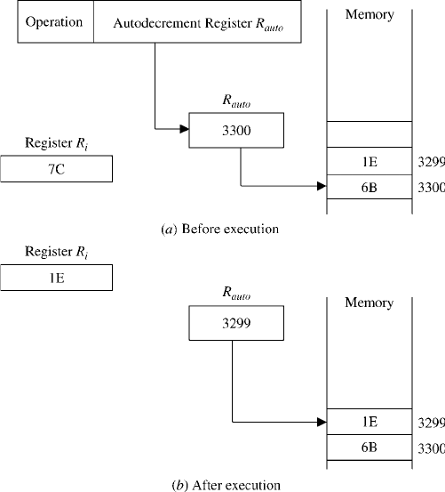
Autodecrement Mode Similar to the autoincrement, the autodecrement mode
uses a register to hold the address of the operand. However, in this case the
content of the autodecrement register is first decremented and the new content
is used as the effective address of the operand. In order to reflect the fact that the
content of the autodecrement register is decrem ented before accessing the operand,
a(2) is include d before the indirection parentheses. Consider, for example, the
instruction LOAD (R
auto
), R
i
. This instruction decrements the content of the
register R
auto
and then uses the new content as the effective address of the operand
that is to be loaded into register R
i
. Figure 2.11 illustrates the autodecrement addres-
sing mode.
The seven addressing modes presented above are summarized in Table 2.2. In
each case, the table shows the name of the addressing mode, its definition, and a gen-
eric example illustrating the use of such mode.
In presenting the different addressing modes we have used the load instruction
for illustration. However, it should be understood that there are other types of
instructions in a given machine. In the following section we elaborate on the differ-
ent types of instructions that typically constitute the instru ction set of a given
machine.
Figure 2.11 Illustration of the autodecrement addressing mode
2.2. ADDRESSING MODES 25

2.3. INSTRUCTION TYPES
The type of instructions forming the instruction set of a machine is an indication of
the power of the underlying architecture of the machine. Instructions can in general
be classified as in the following Subsections 2.3.1 to 2.3.4.
2.3.1. Data Movement Instructions
Data movement instructions are used to move data among the different units of the
machine. Most notably among these are instructions that are used to move data
among the different registers in the CPU. A simple register to register movement
of data can be made through the instruction
MOVE R
i
,R
j
TABLE 2.2 Summary of Addressing Modes
Addressing
mode Definition Example Operation
Immediate Value of operand is included in
the instruction
load #1000, R
i
R
i
1000
Direct
(Absolute)
Address of operand is included
in the instruction
load 1000, R
i
R
i
M[1000]
Register
indirect
Operand is in a memory
location whose address is in
the register specified in the
instruction
load (R
j
), R
i
R
i
M[R
j
]
Memory
indirect
Operand is in a memory
location whose address is in
the memory location
specified in the instruction
load (1000), R
i
R
i
M[1000]
Indexed Address of operand is the sum
of an index value and the
contents of an index register
load X(R
ind
), R
i
R
i
M[R
ind
þ X]
Relative Address of operand is the sum
of an index value and the
contents of the program
counter
load X(PC), R
i
R
i
M[PC þ X]
Autoincrement Address of operand is in a
register whose value is
incremented after fetching
the operand
load (R
auto
)þ, R
i
R
i
M[R
auto
]
R
auto
R
auto
þ 1
Autodecrement Address of operand is in a
register whose value is
decremented before fetching
the operand
load 2 (R
auto
), R
i
R
auto
R
auto
2 1
R
i
M[R
auto
]
26
INSTRUCTION SET ARCHITECTURE AND DESIGN

This instruction moves the content of register R
i
to register R
j
. The effect of the instruc-
tion is to override the contents of the (destination) register R
j
without changing the con-
tents of the (source) register R
i
. Data movement instructions include those used to
move data to (from) registers from (to) memory. These instructions are usually referred
to as the load and store instructions, respectively. Examples of the two instructions are
LOAD 25838, R
j
STORE R
i
, 1024
The first instruction loads the content of the memory location whose address is 25838
into the destination register R
j
. The content of the memory location is unchanged by
executing the LOAD instruction. The STORE instruction stores the content of the
source register R
i
into the memory location 1024. The content of the source register
is unchanged by executing the STORE instruction. Table 2.3 shows some common
data transfer operations and their meanings.
2.3.2. Arithmetic and Logical Instructions
Arithmetic and logical instructions are those used to perform arithmetic and logical
manipulation of registers and memory contents. Examples of arithmetic instructions
include the ADD and SUBTRACT instructions. These are
ADD R
1
,R
2
,R
0
SUBTRACT R
1
,R
2
,R
0
The first instruction adds the content s of source registers R
1
and R
2
and stores the
result in destination register R
0
. The second instruction subtracts the contents of
the source registers R
1
and R
2
and stores the result in the destination register R
0
.
The contents of the source registers are unchanged by the ADD and the SUBTRACT
instructions. In addi tion to the ADD and SUBTRACT instructions, some machines
have MULTIPLY and DIVIDE instructions. These two instructions are expensive
to implement and could be substituted by the use of repeated addition or repeated
subtraction. Therefore, most modern architectures do not have MULTIPLY or
TABLE 2.3 Some Common Data Movement Operations
Data movement
operation Meaning
MOVE Move data (a word or a block) from a given source
(a register or a memory) to a given destination
LOAD Load data from memory to a register
STORE Store data into memory from a register
PUSH Store data from a register to stack
POP Retrieve data from stack into a register
2.3. INSTRUCTION TYPES 27

DIVIDE instructions on their instruction set. Table 2.4 shows some common arith-
metic operations and their meanings.
Logical instructions are used to perform logical operations such as AND, OR,
SHIFT, COMPARE, and ROTATE . As the names indicate, these instructions per-
form, respectively, and, or, shift, compare, and rotate operations on regi ster or
memory contents. Table 2.5 presents a number of logical operations.
2.3.3. Sequencing Instructions
Control (sequencing) instructions are used to change the sequence in which
instructions are executed . They take the form of CONDITIONAL BRANCHING
(CONDITIONAL JUMP), UNCONDITIONAL BRANCHING (JUMP), or CALL
instructions. A common characteristic among these instructions is that their
execution changes the program counter (PC) value. The change made in the PC
value can be unconditional, for example, in the unconditional branching or the
jump instructions. In this case, the earlier value of the PC is lost and execution of
the program starts at a new value specified by the instruction. Consider, for example,
the instruction JUMP NEW-ADDRESS. Execution of this instruction will cause the
PC to be loaded with the memory location represented by NEW-ADDRESS
whereby the instruction stored at this new address is executed. On the other hand,
TABLE 2.4 Some Common Arithmetic Operations
Arithmetic operations Meaning
ADD Perform the arithmetic sum of two operands
SUBTRACT Perform the arithmetic difference of two operands
MULTIPLY Perform the product of two operands
DIVIDE Perform the division of two operands
INCREMENT Add one to the contents of a register
DECREMENT Subtract one from the contents of a register
TABLE 2.5 Some Common Logical Operations
Logical operation Meaning
AND Perform the logical ANDing of two operands
OR Perform the logical ORing of two operands
EXOR Perform the XORing of two operands
NOT Perform the complement of an operand
COMPARE Perform logical comparison of two operands and
set flag accordingly
SHIFT Perform logical shift (right or left) of the content
of a register
ROTATE Perform logical shift (right or left) with
wraparound of the content of a register
28
INSTRUCTION SET ARCHITECTURE AND DESIGN

the change made in the PC by the branching instruction can be conditional based on
the value of a specific flag. Examples of these flags include the Negative (N), Zero
(Z), Overflow (V), and Carry (C). These flags represent the individual bits of a
specific register, called the CONDITION CODE (CC) REGISTER. The values of
flags are set based on the results of executing different instructions. The meaning
of each of these flags is show n in Table 2.6.
Consider, for example, the following group of instructions.
LOAD # 100, R
1
Loop: ADD (R
2
) þ , R
0
DECREMENT R
1
BRANCH-IF-GREATER-THAN Loop
The fourth instruction is a conditional branch instruction, which indicates that if
the result of decrementing the contents of register R
1
is greater than zero, that is,
if the Z flag is not set, then the next instruction to be executed is that labeled by
Loop. It should be noted that conditional branch instructions could be used to exe-
cute program loops (as shown above).
The CALL instructions are used to cause execution of the program to transfer to a
subroutine. A CALL instruction has the same effect as that of the JUMP in terms of
loading the PC with a new value from which the next instruction is to be executed.
However, with the CALL instruction the incremented value of the PC (to point to the
next instruction in sequence) is pushed onto the stack. Execution of a RETURN
instruction in the subroutine will load the PC with the popped value from the
stack. This has the effect of resuming program execution from the point where
branching to the subroutine has occurred.
Figure 2.12 shows a program segment that uses the CALL instruction. This pro-
gram segment sums up a number of values, N, and stores the result into memory
location SUM. The values to be added are stored in N consecutive memory locations
starting at NUM. The subroutine, called ADDITION, is used to perform the actual
addition of values while the main program stores the results in SUM.
Table 2.7 presents some common transfer of control operations.
TABLE 2.6 Examples of Condition Flags
Flag name Meaning
Negative (N) Set to 1 if the result of the most recent operation
is negative, it is 0 otherwise
Zero (Z) Set to 1 if the result of the most recent operation
is 0, it is 0 otherwise
Overflow (V) Set to 1 if the result of the most recent operation
causes an overflow, it is 0 otherwise
Carry (C) Set to 1 if the most recent operation results in a
carry, it is 0 otherwise
2.3. INSTRUCTION TYPES 29

2.3.4. Input/Output Instructions
Input and output instructions (I/ O instructions) are used to transfer data between the
computer and peripheral devices. The two basic I/O instructions used are the INPUT
and OUTPUT instructions. The INPUT instruction is used to transfer data from an
input device to the processor. Examples of input devices include a keybo ard or a
mouse. Input devices are interfaced with a computer through dedicated input
ports. Computer s can use dedicated addresses to address these ports. Suppose that
the input port through which a keyboard is connected to a compute r carries the
unique address 1000. Therefore, execution of the instruction INPUT 1000 will
cause the data stored in a specific register in the interface between the keyboard
and the computer, call it the input data register, to be moved into a specific register
(called the accumulator) in the computer. Similarly, the execution of the instruction
OUTPUT 2000 causes the data stored in the accumulator to be moved to the data
output register in the outpu t device whose address is 2000. Alternatively, the com-
puter can address these ports in the usual way of addressing memory locations. In
this case, the computer can input data from an input device by executing an instruc-
tion such as MOVE R
in
, R
0
. This instruction moves the content of the register R
in
into the register R
0
. Similarly, the instruction MOVE R
0
, R
in
moves the contents
of register R
0
into the register R
in
, that is, performs an output operation. This
CLEAR R
0
MOVE N,R
1
MOVE #NUM,R
2
CALL SUBROUTINE ADDITION
MOVE R
0
, SUM
SUBROUTINE ADDITION
Loop:
ADD (R
2
)+,R
0
DEC R
1
BRANCH-IF-GREATER Loop
RETURN ADDITION
Figure 2.12 A program segment using a subroutine
TABLE 2.7 Some Transfer of Control Operations
Transfer of control operation Meaning
BRANCH-IF-CONDITION Transfer of control to a new address if condition is true
JUMP Unconditional transfer of control
CALL Transfer of control to a subroutine
RETURN Transfer of control to the caller routine
30
INSTRUCTION SET ARCHITECTURE AND DESIGN
latter scheme is called memory-mapped Input/Output. Among the advantages of
memory-mapped I/O is the ability to execute a number of memory-dedicated
instructions on the registers in the I/O devices in addition to the elimination of
the need for dedicated I/O instru ctions. Its main disadvantage is the need to dedicate
part of the memory address space for I/O devices.
2.4. PROGRAMMING EXAMPLES
Having introdu ced addressing modes and instruction types, we now move on to
illustrate the use of these concepts through a number of programming examples.
In presenting these examples, generic mnemonics will be used. This is done in
order to emphasize the understanding of how to use different addressing modes in
performing different operations independent of the machine used. Applications of
similar principles using real-life machine examples are presented in Chapter 3.
Example 1 In this example, we would like to show a program segment that can be
used to perform the task of adding 100 numbers stored at consecutive memory loca-
tions starting at location 1000. The results should be stored in memory location 2000.
CLEAR R
0
; R
0
0
MOVE # 100, R
1
; R
1
100
CLEAR R
2
; R
2
0
LOOP: ADD 1000(R
2
), R
0
; R
0
R
0
þ M (1000 þ R
2
)
INCREMENT R
2
; R
2
R
2
þ 1
DECREMENT R
1
; R
1
R
1
1
BRANCH-IF . 0LOOP; GO TO LOOP if contents of R
1
. 0
STORE R
0
, 2000; M(2000) R
0
In this example, use has been made of immediate (MOVE #100, R
1
)andindexed(ADD
1000(R
2
), R
0
) addressing.
Example 2 In this example autoincrement addressing will be used to perform the
same task performed in Example 1.
CLEAR R
0
; R
0
0
MOVE #100, R
1
; R
1
100
CLEAR R
2
; R
2
0
LOOP: ADD 1000(R
2
)þ, R
0
; R
0
R
0
þ M (1000 þ R
2
) & R
2
R
2
þ 1
DECREMENT R
1
; R
1
R
1
1
BRANCH-IF . 0 LOOP; GO TO LOOP if contents of R
1
. 0
STORE R
0
, 2000; M(2000) R
0
As can be seen, a given task can be performed using more than one programming
methodology. The method used by the programmer depends on his/her experience
2.4. PROGRAMMING EXAMPLES 31

as well as the richness of the instruction set of the machine used. Note also that the
use of the autoincrement addressing in Example 2 has led to a decrease in the
number of instructions used to perform the same task.
Example 3 This example illustrates the use of a subroutine, SORT, to sort
N values in ascending order (Fig. 2.13). The numbers are originally stored in a
list starting at location 1000. The sorted values are also stored in the same list
and again starting at location 1000. The subroutine sorts the data using the well-
known “B ubble Sort” technique. The content of register R
3
is checked at the end
of every loop to find out whether the list is sorted or not.
Example 4 This exam ple illustrates the use of a subroutine, SEARCH, to search
for a value VAL in a list of N values (Fig. 2.14). We assume that the list is not orig-
inally sorted and therefore a brute force search is used. In this search, the value VAL
is compared with every element in the list from top to bottom. The content of register
R
3
is used to indicate whether VAL was found. The first element of the list is located
at address 1000.
Example 5 This exam ple illustrates the use of a subroutine, SEARCH, to search
for a value VAL in a list of N values (as in Example 4) (Fig. 2.15). Here, we make use
of the stack to send the parameters VAL and N .
Figure 2.13 SORT subroutine
32
INSTRUCTION SET ARCHITECTURE AND DESIGN

2.5. SUMMARY
In this chapter we considered the main issues relating to instruction set design and
characteristics. We presented a model of the main memory in which the memory is
abstracted as a sequence of cells, each capable of storing n bits. A number of addressing
modes were presented. These include immediate, direct, indirect, indexed, autoincre-
ment, and autodecrement. Examples showing how to use these addressing modes
were then presented. We also presented a discussion on instruction types, which include
data movement, arithmetic/logical, instruction sequencing, and Input/Output. Our dis-
cussion concluded with a presentation of a number of examples showing how to use the
principles and concepts discussed in the chapter in programming the solution of a
number of sample problems. In the next chapter, we will introduce the concepts involved
in programming the solution of real-life problems using assembly language.
Figure 2.14 SEARCH subroutine
Figure 2.15 Subroutine SEARCH using stack to send parameters VAL and N
2.5. SUMMARY 33
EXERCISES
1. Write a program using the addressing modes and the instruction types pre-
sented in Sections 2.2 and 2.3 to reverse the bits stored in a 16-bit register R
0
.
2. Consider a computer that has a number of registers such that the three reg-
isters R
0
¼ 1500, R
1
¼ 4500, and R
2
¼ 1000. Show the effective address
of memory and the registers’ contents in each of the following instructions
(assume that all numbers are decimal).
(a) ADD (R
0
)þ, R
2
(b) SUBTRACT 2 (R
1
), R
2
(c) MOVE 500(R
0
), R
2
(d) LOAD #5000, R
2
(e) STORE R
0
, 100(R
2
)
3. Assume that the top of the stack in a program is pointed to by the register SP.
You are required to write program segments to perform each of the following
tasks (assume that only the following addressing modes are available:
indexed, autoincrement, and autodecrement).
(a) Pop the top three elements of the stack, add them, and push the result
back onto the stack.
(b) Pop the top two elements of the stack, subtract them, and push the results
back onto the stack.
(c) Push five elements (one at a time) onto the stack.
(d) Remove the top five elements from the top of the stack.
(e) Copy the third element from the top of the stack into register R
0
.
4. You are required to write a program segment that can perform the operation
C A þ B where each of A and B represents a set of 100 memory locations
each storing a value such that the set of values represented by A are stored
starting at memory location 1000 and those represented by B are stored start-
ing at memory location 2000. The results should be stored starting at memory
location 3000. The above operation is to be performed using each of the
following instruction classes.
(a) A machine with one-address instructions
(b) A machine with one-and-half instructions
(c) A machine with two-address instructions
(d) A machine with three-address instructions
(e) A machine with zero-address instructions
5. Write program segments that perform the operation C C þ A B using
each of the instruction classes indicated in Ex ercise 4 above. Assume that
A, B, and C are memor y addre sses.
6. Assume that a series of five tests has been offered to a class consisting of 50
students. The score obtained by students in each of the five tests are stored
sequentially in memory locations starting respectively at memory locations
1000, 2000, 3000, 4000, and 5000. You are required to write a program
34 INSTRUCTION SET ARCHITECTURE AND DESIGN
that calculates the average score obtained by each student in the five tests and
store the same in memory locations starting at memory location 6000. Each
student is identified by his/her student ID. You may assume that students’
IDs are sequential.
7. Repeat Exercise 6 above assuming that the memory used is byte addressable
while each score occupies 32-bit.
8. Rewrite the same program as in Exercise 6 above assuming that the students’
IDs are not sequential, that is, each student ID is to be used as a pointer to
his/her test scores.
9. Repeat Exercise 6 above assuming that the students scores are stored in an
array S(50,5), that is, each row holds the scor es obtained by a student
(each score in a column of the same row) and that the first element of the
array, that is, S (0,0) is stored in memory location 4000. The scores are
stored rowwise, that is, one row after the other. The average score obtained
by each student is to be stored at a memor y location pointed to by his/her ID.
10. Repeat Exercise 9 above assumi ng that your job is to write a subroutine
to perform the same task as in Exercise 9. Assume that the number of
students, the number of tests, and the location of the first element in the
array are to be passed to the subroutine as parameters in registers R
1
, R
2
,
and R
3
, respectively.
REFERENCES AND FURTHER READING
C. M. Gilmore, Microprocessors: Principles and Applications, 2nd ed., McGraw-Hill,
New York, 1996.
V. C. Hamacher, Z. G. Vranesic, and S. G. Zaky, Computer Organization, 5th ed.,
McGraw-Hill, New York, 2002
A. D. Patterson, J. L. Hennessy, Computer Organization & Design; The Hardware/Software
Interface, Morgan Kaufmann, San Mateo, CA, 1994
B. Wilkinson, Computer Architecture: Design and Performance, 2nd ed., Prentice-Hall,
Hertfordshire, UK, 1996.
REFERENCES AND FURTHER READING 35

&
CHAPTER 3
Assembly Language Programming
In Chapter 2 we introduced the basic concepts and principles involved in the design
of an instruction set of a machine. This chapter considers the issues related to asse m-
bly language programming. Although high-level languages and compiler technol-
ogy have witnessed great advances over the years, assembly lang uage remains
necessary in some cases. Programming in assembly can result in machine code
that is much smaller and much faster than that generated by a compiler of a high-
level language. Small and fast code could be critical in some embedded and portable
applications, where resources may be very limited. In such cases, small portions of
the program that may be heavily used can be written in assembly lang uage. For the
reader of this book, learning assembly languages and writing assembly code can be
extremely helpful in understanding computer organization and architecture.
A computer program can be represented at different levels of abstraction. A pro-
gram could be written in a machine-i ndependent, high-level language such as Java
or Cþþ. A computer can execute programs only when they are represented in
machine language specific to its architecture. A machine language program for a
given architecture is a collection of machine instructions represented in binary
form. Programs written at any level higher than the machine language must be trans-
lated to the binary representation before a computer can execute them. An assembly
language program is a symbolic representation of the machine language program.
Machine language is pure binary code, whereas assembly language is a direct map-
ping of the binary code onto a symbolic form that is easier for humans to understand
and manage. Converting the symbolic representation into machine language is per-
formed by a special program called the assembler . An assembler is a program that
accepts a symbolic language program (source) and produces its machine language
equivalent (target). In translating a program into binary code, the assembler will
replace sym bolic addresses by numeric addresses, replace symbolic operation
codes by machine operation codes, reserve storage for instructions and data, and
translate constants into machine representation.
The purpose of this chapter is to give the reader a general overview of assembly
language and its programming. It is not meant to be a manual of the assembly
language for any specific architecture. We start the chapter with a discussion of a
37
Fundamentals of Computer Organization and Architecture, by M. Abd-El-Barr and H. El-Rewini
ISBN 0-471-46741-3 Copyright # 2005 John Wiley & Sons, Inc.

simple hypothetical machine that will be referred to throughout the chapter. The
machine has only five registers and its instruction set has only 10 instructions.
We will use this simple machine to define a rather simple assembly language that
will be easy to understand and will help explain the main issues in assembly pro-
gramming. We will introduce instruction mnemonics and the syntax and assembler
directives and commands. A discussion on the execution of assembly programs is
then presented. We conclude the chapter by showing a real-world example of the
assembly language for the X86 Intel CISC family.
3.1. A SIMPLE MACHINE
Machine language is the native language of a given processor. Since assembly
language is the symbolic form of machine language, each different type of processor
has its own unique assembly language. Before we study the assembly language of a
given processor, we need first to understand the details of that processor. We need to
know the memory size and organization, the processor registers, the instruction
format, and the entire instruction set. In this section, we present a very simple
hypothetical processor, which will be used in explaining the different topics in
assembly language throughout the chapter.
Our simple machine is an accumulator-based processor, which has five 16-bit
registers: Program Counter (PC), Instruction Register (IR), Address Register
(AR), Accumulator (AC), and Data Register (DR). The PC contains the address
of the next instruction to be executed. The IR contains the operation code portion
of the instruction being executed. The AR contains the address portion (if any) of
the instruction being executed. The AC serves as the implicit source and destination
of data. The DR is used to hold data. The memory unit is made up of 4096 words of
storage. The word size is 16 bits. The processor is shown in Figure 3.1.
CPU
ALU
Figure 3.1 A simple machine
38
ASSEMBLY LANGUAGE PROGRAMMING

We assume that our simple processor supports three types of instructions : data
transfer, data processing, and program control. The data transfer operations are
load, store, and move data between the registers AC and DR. The data processing
instructions are add, subtract, and, and not. The program control instructions are
jump and conditional jump. The instruction set of our processor is summarized in
Table 3.1. The instruction size is 16 bits, 4 bits for the operation code and 12 bits
for the address (when appropriate).
Example 1 Let us write a machine language program that adds the contents of
memory location 12 (00C-hex), initialized to 350 and memory location 14 (00E-hex),
initialized to 96, and store the result in location 16 (010-hex), initialized to 0.
The program is given in binary instructions in Table 3.2. The first column gives
the memory location in binary for each instruction and operand. The second column
TABLE 3.1 Instruction Set of the Simple Processor
Operation code Operand Meaning of instruction
0000 Stop execution
0001 adr Load operand from memory (location adr) into AC
0010 adr Store contents of AC in memory (location adr)
0011 Copy the contents AC to DR
0100 Copy the contents of DR to AC
0101 Add DR to AC
0110 Subtract DR from AC
0111 And bitwise DR to AC
1000 Complement contents of AC
1001 adr Jump to instruction with address adr
1010 adr Jump to instruction adr if AC ¼ 0
TABLE 3.2 Simple Machine Language Program in Binary (Example 1)
Memory location
(bytes) Binary instruction Description
0000 0000 0000 0001 0000 0000 1100 Load the contents of location 12 in AC
0000 0000 0010 0011 0000 0000 0000 Move contents of AC to DR
0000 0000 0100 0001 0000 0000 1110 Load the contents of location 14 into AC
0000 0000 0110 0101 0000 0000 0000 Add DR to AC
0000 0000 1000 0010 0000 0001 0000 Store contents of AC in location 16
0000 0000 1010 0000 0000 0000 0000 Stop
0000 0000 1100 0000 0001 0101 1110 Data value 350
0000 0000 1110 0000 0000 0110 0000 Data value is 96
0000 0001 0000 0000 0000 0000 0000 Data value is 0
3.1. A SIMPLE MACHINE 39

lists the contents of the memory locations. For example, the contents of location 0 is
an instruction with opcode: 0001, and operand address: 0000 0000 1100. Please note
that in the case of operations that do not require operand, the operand portion of the
instruction is shown as zeros. The program is expected to be stored in the indicated
memory locations starting at location 0 during execution. If the program will be
stored at different memory locations, the addresses in some of the instructions
need to be updated to reflect the new locations.
It is clear that programs written in binary code are very difficult to understand
and, of course, to debug. Representing the instructions in hexadecimal will reduce
the number of digits to only four per instruction. Table 3.3 show s the same program
in hexadecimal.
3.2. INSTRUCTION MNEMONICS AND SYNTAX
Assembly language is the symbolic form of machine language. Assembly programs
are written with short abbreviations called mnemonics. A mnemonic is an abbrevi-
ation that represents the actual machine instruction. Assembly language program-
ming is the writing of machine instructions in mnemonic form, where each
machine instruction (binary or hex value) is replaced by a mnemonic. Clearly the
use of mnemonics is more meaningful than that of hex or binary values, which
would make programming at this low level easier and more manageable.
An assembly program consists of a sequence of assembly statements, where
statements are written one per line. Each line of an assembly program is split into
the following four fields: label, operation code (opcode), operand, and comments.
Figure 3.2 shows the four-column format of an assembly instruction.
Labels are used to provide symbolic names for memory addresses. A label is an
identifier that can be used on a program line in order to branch to the labeled line. It
can also be used to access data using symbolic names. The maximum leng th of a
TABLE 3.3 Simple Machine Language Program in
Hexadecimal (Example 1)
Memory location
(bytes) Hex instruction
000 100C
002 3000
004 100E
006 5000
008 2010
00A 0000
00C 015E
00E 0060
010 0000
40
ASSEMBLY LANGUAGE PROGRAMMING

label differs from one assembly language to another. Some allow up to 32 charact ers
in length, others may be restricted to six characters. Assembly languages for some
processors require a colon after each label while others do not. For example, SPARC
assembly requires a colon after every label, but Motorola assembly does not. The
Intel assembly requires colons after code labels but not after data labels.
The operation code (opcode) field contains the symbolic abbreviation of a given
operation. The operand field consists of additional information or data that the
opcode requires. The operand field may be used to specify constant, label, immedi-
ate data, register, or an address. The comments field provides a space for documen-
tation to explain what has been done for the purpose of debugging and maintenance.
For the simple processor described in the previous section, we assume that the
label field, which may be empty, can be of up to six characters. There is no colon
requirement after each label. Comments will be preceded by “/”. The simple
mnemonics of the ten binary instructions of Table 3.1 are summarized in Table 3.4.
Let us consider the following assembly instruction:
START LD X \ copy the contents of location X into AC
The label of the instruction LD X is START, which means that it is the memory
address of this instruction. That label can be used in a program as a refere nce as
shown in the following instruction:
BRA START \ go to the statement with label START
Label
(Optional)
Operation Code
(Required)
Operand
(Required in some
instructions)
Comment
(Optional)
Figure 3.2 Assembly instruction format
TABLE 3.4 Assembly Language for the Simple Processor
Mnemonic Operand Meaning of instruction
STOP Stop execution
LD x Load operand from memory (location x) into AC
ST x Store contents of AC in memory (location x)
MOVAC Copy the contents AC to DR
MOV Copy the contents of DR to AC
ADD Add DR to AC
SUB Subtract DR from AC
AND And bitwise DR to AC
NOT Complement contents of AC
BRA adr Jump to instruction with address adr
BZ adr Jump to instruction adr if AC ¼ 0
3.2. INSTRUCTION MNEMONICS AND SYNTAX 41
The jump instruction will make the processor jump to the memory address associ-
ated with the label START, thus executing the instruction LD X immediately
after the BRA instruction.
In addition to program instructions, an assembly progr am may also include
pseudo instructions or assembler directives. Assembler directives are commands
that are understood by the assembler and do not correspond to actual machine
instructions. For example, the assembler can be asked to allocate memory storage.
In our assembly language for the simple processor, we assume that we can use
the pseudo instru ction W to reserve a word (16 bits) in memory. For example,
the following pseudo instruction reserves a word for the label X and initializing
it to the decimal value 35 0:
X W 350 \ reserve a word initialized to 350
Again, the label of the pseudo instruction W 350 is X, which means it is the memory
address of this value. The following is the assembly code of the machine language
program of Example 1 in the previous section.
LD X \ AC X
MOVAC \ DR AC
LD Y \ AC Y
ADD \ AC AC þ DR
ST Z \ Z AC
STOP
X W 350 \ reserve a word initialized to 350
Y W 96 \ reserve a word initialized to 96
Z W 0 \ result stored here
Example 2 In this example, we will write an assembly program to perform
the multiplication operatio n: Z X
Y, where X, Y, and Z are memory
locations.
As you know, the assembly of the simple CPU does not have a multiplication
operation. We will compute the product by applying the add operation multiple
times. In order to add Y to itself X times, we will use N as a counter that is initialized
to X and decremented by one after each addition step. The BZ instruction will be
used to test for the case when N reaches 0. We will use a memory location to
store N but it will need to be loaded into AC before the BZ instruction is executed.
We will also use a memory location ONE to store the constant 1. Memory location Z
will have the partial products and eventually the final result.
The following is the assembly program using the assembly language of
our simple processor. We will assume that the values of X and Y are
small enough to allow their product to be stored in a single word. For the
sake of this example, let us assume that X and Y are initialized to 5 and 15,
respectively.
42 ASSEMBLY LANGUAGE PROGRAMMING
LD X \ Load X in AC
ST N \ Store AC (X original value) in N
LOOP LD N \ AC N
BZ EXIT \ Go to EXIT if AC ¼ 0 (N reached 0)
LD ONE \ AC 1
MOVAC \ DR AC
LD N \ AC N
SUB \ subtract 1 from N
ST N \ store decrements N
LD Y \ AC Y
MOVAC \ DR AC
LD Z \ AC Z (partial product)
ADD \ Add Y to Z
ST Z \ store the new value of Z
BRA LOOP
EXIT STOP
X W 5 \ reserve a word initialized to 5
Y W 15 \ reserve a word initialized to 15
Z W 0 \ reserve a word initialized to 0
ONE W 1 \ reserve a word initialized to 1
N W 0 \ reserve a word initialized to 0
3.3. ASSEMBLER DIRECTIVES AND COMMANDS
In the previous section, we introduced the reader to assembly and machine languages.
We provided several assembly code segments written using our simple machine
model. In writing assembly language programs for a specific architecture, a number
of practical issues need to be considered. Among these issues are the following:
.
Assembler directives
.
Use of symbols
.
Use of synthetic operations
.
Assembler syntax
.
Interaction with the operating system
The use of assembler directives, also called pseudo-operations, is an important issue
in writing assembly language programs. Assembler directives are commands that
are understood by the assembler and do not correspond to actual machine instruc-
tions. Assembler directives affect the way the assembler performs the conversion
of assembly code to machine code. For example, special assembler directives can
be used to instruct the assembler to place data items such that they have proper align-
ment. Align ment of data in memory is required for efficient implementation of archi-
tectures. For proper alignment of data, data of n-bytes width must be stored at an
3.3. ASSEMBLER DIRECTIVES AND COMMANDS 43

address that is divisible by n, for example, a word that has a two-byte width has to be
stored at locations having addresses divisible by two.
In assembly language programs symbols are used to represent numbers, for
example, immediate data. This is done to make the code easier to read, understand,
and debug. Symbols are translated to their corresponding numerical values by the
assembler.
The use of synthetic operations helps assembly programmers to use instructions
that are not directly suppor ted by the architecture. These are then translated by the
assembler to a set of instructions defined by the architecture. For example, assem-
blers can allow the use of (a synthetic) increment instruction on architectures for
which an increment instruction is not defined through the use of some other instruc-
tions such as the add instruction.
Assemblers usually impose some conventions in referring to hardware com-
ponents such as registers and memory locations. One such convention is the prefix-
ing of immediate values with the special characters (#) or a register name with the
character (%).
The underlying hardware in some machines cannot be accessed directly by a pro-
gram. The operating system (OS) plays the role of mediating access to resources
such as memory and I/O facilities. Interactions wi th operating systems (OS) can
take place in the form of a code that causes the execution of a function that is
part of the OS. These functions are called system calls.
3.4. ASSEMBLY AND EXECUTION OF PROGRAMS
As you know by now, a program written in assembly language needs to be trans-
lated into binary machine language before it can be executed. In this section, we
will learn how to get from the point of writing an assembly program to the
execution phase. Figure 3.3 shows three steps in the assembly and execution pro-
cess. The assembler reads the source program in assembly language and generates
the object program in binary form. The object program is passed to the linker. The
linker will check the object file for calls to procedures in the link library. The linker
will combine the required procedures from the link library with the object program
and produce the executable program. The loader loads the executable program into
memory and branches the CPU to the starting address. The program begins
execution.
Figure 3.3 Assembly and execution process
44
ASSEMBLY LANGUAGE PROGRAMMING

3.4.1. Assemblers
Assemblers are programs that generate machine code instructions from a source
code program written in assembly language. The assembler will replace symbolic
addresses by numeric addresses, replace symbolic operation codes by machin e oper-
ation codes, reserve storage for instructions and data, and translate constants into
machine representation.
The functions of the assembler can be performed by scanning the assembly pro-
gram and mapping its instructions to their machine code equivalent. Since symbols
can be used in instructions before they are defined in later ones, a single scanning of
the program might not be enough to perform the mapping. A simple assembler scans
the entire assembly program twice, where each scan is called a pass. During the first
pass, it generates a table that includes all sym bols and their binary values. This table
is called the symbol table. During the second pass, the assembler will use the symbol
table and other tables to generate the object program, and output some information
that will be needed by the linker.
3.4.2. Data Structures
The assembler uses at least three tables to perform its functions: symbol table,
opcode table, and pseudo instruction table. The symbol table, which is generated
in pass one, has an entry for every symbol in the program. Associated with each
symbol are its binary value and other information. Table 3.5 shows the symbol
table for the multiplication program segment of Example 2. We assume that the
instruction LD X is starting at location 0 in the memory. Since each instruction
takes two bytes, the value of the symbol LOOP is 4 (004 in hexadecimal).
Symbol N, for example, will be stored at decimal location 40 (028 in hexadecimal).
The values of the other symbols can be obtained in a similar way.
The opcode table provides information about the operation codes. Associated
with each symbolic opcode in the table are its numerical value and other information
about its type, its instruction length, and its operands. Table 3.6 shows the opcode
TABLE 3.5 Symbol Table for the Multiplication
Segment (Example 2)
Symbol
Value
(hexadecimal)
Other
information
Loop 004
EXIT 01E
X 020
Y 022
Z 024
ONE 026
N 028
3.4. ASSEMBLY AND EXECUTION OF PROGRAMS 45

table for the simple processor described in Section 3.1. As an example, we explain
the information associated with the opcode LD. It has one operand, which is a
memory address and its binary value is 0001. The instruction length of LD is
2 bytes and its type is memory-reference.
The entries of the pseudo instruction table are the pseudo instructions symbols.
Each entry refers the assembler to a procedure that processes the pseudo instruction
when encountered in the program. For example, if END is encoun tered, the trans-
lation process is terminated.
In order to keep track of the instruction locations, the assembler maintains a vari-
able called instruction location counter (ILC). The ILC contains the value of
memory location assigned to the instruction or operand being processed. The ILC
is initialized to 0 and is incremented after processing each instruction. The ILC is
incremented by the length of the instruction being processed, or the number of
bytes allocated as a result of a data allocation pseudo instruction.
Figures 3.4 and 3.5 show simplified flowcharts of pass one and pass two in a two-
pass assembler. Remember that the main function of pass one is to build the symbol
table while pass two’s main function is to generate the object code.
3.4.3. Linker and Loader
The linker is the entity that can combine object modules that may have resulted from
assembling multiple assembly modules separately. The loader is the operating
system utility that reads the executable into memory and start execution.
In summary, after assembly modules are translated into object modules, the func-
tions of the linker and loader prepare the program for execution. These functions
include combining object modules together, resolving addresses unknown at assem-
bly time, allocating storage, and finally executing the program.
TABLE 3.6 The Opcode Table for the Assembly of our Simple Processor
Opcode Operand
Opcode value
(binary)
Instruction length
(bytes) Instruction type
STOP — 0000 2 Control
LD Mem-adr 0001 2 Memory-reference
ST Mem-adr 0010 2 Memory-reference
MOVAC — 0011 2 Register-reference
MOV — 0100 2 Register-reference
ADD — 0101 2 Register-reference
SUB — 0110 2 Register-reference
AND — 0111 2 Register-reference
NOT — 1000 2 Register-reference
BRA Mem-adr 1001 2 Control
BZ Mem-adr 1010 2 Control
46
ASSEMBLY LANGUAGE PROGRAMMING

3.5. EXAMPLE: THE X86 FAMILY
In this section, we discuss the assembly language features and use of the X86 family.
We present the basic organizational features of the system, the basic programming
model, the addressing modes, sample of the different instruction types used, and
Start
END
Process next instruction
Stop
No
Yes
Opcode Lookup
Symbol Table Lookup
Generate machine code
Figure 3.5 Simplified pass two in a two-pass assembler
Start
END
Label
ILC ← 0
Process next instruction
Increment ILC
Add to Symbol Table
with value = ILC
Pass 2
No
No
Yes
Yes
Figure 3.4 Simplified pass one in a two-pass assembler
3.5. EXAMPLE: THE X86 FAMILY 47

finally examples showing how to use the assembly language of the system in
programming sample real-life problems.
In the late 1970s, Intel introduced the 8086 as its first 16-bit microp rocessor.
This processor has a 16-bit external bus. The 8086 evolved into a series of faster
and more powerful processors starting with the 80286 and ending with the Pentium.
The latter was introduced in 1993. This Intel family of processors is usually calle d
the X86 family. Table 3.7 summarizes the main features of the main members of
such a family.
The Intel Pentium processor has about three million transistors and its compu-
tational power ranges between two and five times that of its predecessor processor,
the 80486. A number of new features were introduced in the Pentium processor,
among which is the incorporation of a dual-pipelined superscalar architecture
capable of processing more than one instruction per clock cycle.
The basic programming model of the 386, 486, and the Pentium is shown in
Figure 3.6. It consists of three register groups. These are the general purpose regis-
ters, the segment registers, and the instruction pointer (program counter) and the flag
register. The first set consists of general purpose registers A, B, C, D, SI (source
index), DI (des tination index), SP (stack pointer), and BP (base pointer). It should
be noted that in naming these registers, we used X to indicate eXtended. The
second set of registers consists of CS (code segment), SS (stack segment), and
four data segment registers DS, ES, FS, and GS. The third set of registers consists
of the instruction pointer (program counter) and the flags (st atus) register. The
latter is shown in Figure 3.7. Among the status bits shown in Figure 3.7, the first
five are identical to those bits introduced as early as in the 8085 8-bit microproces-
sor. The next 6 – 11 bits are identical to those introduced in the 8086. The flags in the
bits 12–14 were introduced in the 80286 while the 16 –17 bits were introduced in
the 80386. The flag in bit 18 was introduced in the 80486. Table 3.8 shows the mean-
ing of those flags.
In the X86 family an instruction can perform an operation on one or two oper-
ands. In two-operand instructions, the second operand can be immediate data in
TABLE 3.7 Main Features of the Intel X86 Microprocessor Family
Feature 8086 286 386 486 Pentium
Date introduced 1978 1982 1985 1991 1993
Data bus 8 bits 16 bits 32 bits 32 bits 64 bits
Address bus 20 bits 24 bits 32 bits 32 bits 32 bits
Operating speed 5,8,10 MHz 6,8,10, 12.5,
16, 20 MHz
16, 20,25, 33,
40, 50 MHz
25, 33,
50 MHz
50, 60, 66,
100 MHz
Instruction cache
size
NA NA 16 bytes 32 bytes 8 Kbytes
Data cache size NA NA 256 bytes 8 Kbytes 8 Kbytes
Physical memory 1 Mbytes 16 Mbytes 4 Gbytes 4 Gbytes 4 Gbytes
Data word size 16 bits 16 bits 16 bits 32 bits 32 bits
48 ASSEMBLY LANGUAGE PROGRAMMING

Figure 3.6 The base register sets of the X86 programming model
31 18 17 16 15 14 13 12 11 10 9 8 1
Reserved AG VM RF 0 NT IOPL
6543 2 0
ODITSZ A P C
7
Figure 3.7 The X86 flag register
TABLE 3.8 X86 Status Flags
Flag Meaning Processor Flag Meaning Processor
C Carry All P Parity All
A Auxiliary All Z Zero All
S Sign All T Trap All
I Interrupt All D Direction All
O Overflow All IOPL I/O privilege level 286
NT Nested task 286 RF Resume 386
VM Virtual mode 386 AC Alignment check 486
3.5. EXAMPLE: THE X86 FAMILY 49

2’s complement format. Data transfer, arithmetic and logical instructions can act on
immediate data, registers, or memory locations.
In the X86 family, direct and indirect memory addressing can be used. In direct
addressing, a displacement address consisting of a 8-, 16-, or 32-bit word is used as
the logical address. This logical address is added to the shifted contents of the seg-
ment register (segment base address) to give a physical memory address. Figure 3.8
illustrates the direct addressing process.
Address indirection in the X86 family can be obtained using the content of a
base pointer register (BPR), the content of an index register, or the sum of a base
register and an index register. Figure 3.9 illustrates indirect addressing using
the BPR.
The X86 family of processors defines a number of instruction types. Using the
naming convention introduced before, these instru ction types are data movement,
arithmetic and logic, and sequencing (control transfer). In addition, the X86
family defines other instruction types such as string manipulat ion, bit manipulation,
and high-level language support.
Data movement instru ctions in the X86 family include mainly four subtypes.
These are the general-purpose, accumulator-specific, address-object, and flag
instructions. A sample of these instructions is shown in Table 3.9.
Arithmetic and logic instructions in the X86 family include mainly five subtypes.
These are addition, subtraction, multiplication, division, and logic instructions.
A sample of the arithmetic instructions is shown in Table 3.10.
Logic instructions include the typical AND, OR, NOT, XOR, and TEST. The latter
performs a logic compare of the source and the destination and sets the flags accord-
ingly. In addition, the X86 family has a set of shift and rotate instructions. A sample
of these is shown in Table 3.11.
Original 16 bits
7/15/31 15 0
Op Code Address
Segment base
Address
Σ
Physical Address
Displacement from
2
nd
word of instruction
Shifted 16 bits
Logical Address
0
Figure 3.8 Direct addressing in the X86 family
50
ASSEMBLY LANGUAGE PROGRAMMING

Control transfer instructions in the X86 family include mainly four subtypes.
These are conditional, iteration, interrupt, and unconditional. A sample of these
instructions is shown in Table 3.12.
Processor control instructions in the X86 family include mainly three subtypes.
These are external synchronization, flag manipulation, and general control instruc-
tions. A sample of these instructions is shown in Table 3.13.
Having introduced the basic features of the instruction set of the X86 processor
family, we now move on to present a number of programming examples to show
Shifted 16 bits
2
nd
word of instruction
Original 16 bits
7/15/31 0 15 0
Op Code Address
Logical Address
Segment base
Address
Physical AddressBPR
å
å
Displacement from
Figure 3.9 Indirect addressing using BPR in the X86 family
TABLE 3.9 Sample of the X86 Data Movement Instructions
Mnemonic Operation Subtype
MOV Move source to destination General purpose
POP Pop source from stack General purpose
POPA Pop all General purpose
PUSH Push source onto stack General purpose
PUSHA Push all General purpose
XCHG Exchange source with destination General purpose
IN Input to accumulator Accumulator
OUT Output from accumulator Accumulator
XLAT Table lookup to translate byte Accumulator
LEA Load effective address in register Address-object
LMSW Load machine status word Address-object
SMSW Store machine status word Address-object
POPF Pop flags off stack Flag
PUSHF Push flags onto stack Flag
3.5. EXAMPLE: THE X86 FAMILY 51

how the instruction set can be used. The examples presented are the same as those
presented at the end of Chapter 2.
Example 3 Adding 100 numbers stored at consecutive memory locations starting
at location 1000, the results should be stored in memory location 2000. LIST is
TABLE 3.10 Sample of the X86 Arithmetic Instructions
Mnemonic Operation Subtype
ADD Add source to destination Addition
ADC Add source to destination with carry Addition
INC Increment operand by 1 Addition
SUB Subtract source from destination Subtraction
SBB Subtract source from destination with borrow Subtraction
DEC Decrement operand by 1 Subtraction
MUL Unsigned multiply source by destination Multiply
IMUL Signed multiply source by destination Multiply
DIV Unsigned division accumulator by source Division
IDIV Signed division accumulator by source Division
TABLE 3.11 Sample of the X86 Shift and Rotate
Instructions
Mnemonic Operation
ROR Rotate right
ROL Rotate left
RCL Rotate left through carry
RCR Rotate right through carry
SAR Arithmetic shift right
SAL Arithmetic shift left
SHR Logic shift right
SHL Logic shift left
TABLE 3.12 Sample of the X86 Control Transfer Instructions
Mnemonic Operation Subtype
SET Set byte to true or false based on condition Conditional
JS Jump if sign Conditional
LOOP Loop if CX does not equal zero Iteration
LOOPE Loop if CX does not equal zero & ZF ¼ 1 Iteration
INT Interrupt Interrupt
IRET Interrupt return Interrupt
JMP Jump unconditional Unconditional
RET Return from procedure Unconditional
52
ASSEMBLY LANGUAGE PROGRAMMING

defined as an array of N elements each of size byte. FLAG is a memory variable used
to indicate whether the list has been sorted or not. The register CX is used as a coun-
ter with the Loop instruction. The Loop instruction decrements the CX register and
branch if the result is not zero. The addressing mode used to access the array List
[BX þ 1] is called based addressing mode. It should be noted that since we are
using BX and BX þ 1 the CX counter is loaded with the value 999 in order not to
exceed the list.
MOV CX, 1000 2 1 ; Counter ¼ CX (1000 2 1)
MOV BX, Offset LIST ; BX pointer to LIST
CALL SORT
......
SORT PROC NEAR
Again: MOV FLAG, 0 ; FLAG 0
Next: MOV AL, [BX]
CMP AL, [BX þ 1] ;Compare current and next values
JLE Skip ;Branch if current , next values
XCHG AL, [BX þ 1] ;If not , Swap the contents of the
MOV [BX þ 1], AL ;current location with the next one
MOV FLAG, 1 ;Indicate the swap
Skip: INC BX ; BX BX þ 1
LOOP Next ;Go to next value
CMP FLAG, 1 ;Was there any swap
JE Again ;If yes Repeat process
RET
SORT ENDP
Example 4 Here we implement the SEARCH algorithm in the 8086 instruction
set. LIST is defined as an array of N elements each of size word. FLAG is a
memory variable used to indicate whether the list has been sorted or not. The register
CX is used as a counter with the loop instruction. The Loop instruction decrements
TABLE 3.13 Sample of the X86 Processor Control Instructions
Mnemonic Operation Subtype
HLT Halt External sync
LOCK Lock the bus External sync
CLC Clear carry flag Flag
CLI Clear interrupt flag Flag
STI Set interrupt flag Flag
INVD Invalidate data cache General control
3.5. EXAMPLE: THE X86 FAMILY 53
the CX register and branch if the result is not zero. The addressing mode used to
access the array List [BX þ 1] is called based addre ssing mode.
MOV CX, 1000 ; Counter ¼ CX 1000
MOV BX, Offset
LIST
;BX pointer to LIST
MOV SI, 0 ; SI used as an index
MOV AX, VAL ; AX VAL
CALL SEARCH
; Test FLAG to check whether value found
......
SEARCH PROC NEAR
MOV FLAG, 0 ; FLAG 0
Next: CMP AX, [BX þ SI] ;Compare current value to VAL
JE Found ;Branch if equal
ADD SI, 2 ; SI SI þ 2, next value
LOOP Next ;Go to next value
JMP Not_Found
Found: MOV FLAG, 1 ;Indicate value found
MOV POSITION, SI ;Return index of value in List
Not_Found: RET
SEARCH ENDP
Example 5 This is the same as Example 4 but using the stack features of the X86.
PUSH DS ;See Table 3.9
MOV CX, 1000 ;Counter ¼ CX 1000
MOV BX, OFFSET LIST ;Point to beginning of LIST
PUSH BX
PUSH VAL ;VAL is a word variable
CALL SEARCH
;Test FLAG to check whether value found
;If found get index from SI register
using
POP SI
......
SEARCH PROC NEAR
POP TEMP ;Save IP
POP AX ;AX VAL. Value to search for
POP SI ;SI OFFSET LIST and let BX ¼ SI
54 ASSEMBLY LANGUAGE PROGRAMMING
POP ES ;Make ES ¼ DS (See Table)
CLD ;Set auto-increment mode
REPNE SCASW ;Scan LIST for value in AX if not
found; increment SI by 2,
decrement CX and if; not zero
scan next location in LIST.
;If occurrence found Zero flag
is set
JNZ Not_Found ;If valu e not branch to
Not_Found?
MOV FLAG, 1 ;Yes
SUB SI, BX
PUSH SI ;Save position
Not_Found: PUSH TEMP ;Restore IP
RET
SEARCH ENDP
It should be noted in the above example that when a call to a procedure is
initiated, the IP register is the last value to be pushed on top of the stack. Therefore,
care should be made to avoid altering the value of the IP register. The top of the
stack is thus saved to a tempor ary variable TEMP at procedure entry and restored
before exit.
3.6. SUMMARY
A machine language is a collection of the machine instructions represented in 0s and
1s. Assembly language provides easier to use symbolic representation, in which an
alphanumeric equivalent to machine language is used. There is a one-to-one corre-
spondence between assembly language statements and machine instructions. An
assembler is a progr am that accepts a symbolic language program (source program)
and produces its machine language equivalent (target program). Although assembly
language programming is difficult compared to programming in high-level
languages, it is still important to learn assembly. In some applications, small por-
tions of a program that are heavily used may need to be written in assembly
language. Programming in assembly can result in machine code that is smaller
and faster than that generated by a compiler of a high-level language. Assembly pro-
grammers have access to all the hardw are features of the target machine that might
not be accessible to high-level language programmers. In addition, learning assem-
bly languages can be of great help in under standing the low level details of computer
organization and architecture. In this chapter we provided a general overview of
assembly language and its programming. The programmer view of the X86 Intel
microprocessor family of proce ssors was also introduced as a real-world example.
Examples were then presented showing how to use the X86 instruction set in writing
sample programs similar to those presented in Chapter 2.
3.6. SUMMARY 55
EXERCISES
1. What is the difference between each of the following pairs?
.
Compilers and assemblers
.
Source code and target code
.
Mnemonics and hexadecimal representation
.
Pseudo instructions and instructions
.
Labels and addresses
.
Symbol table and opcode table
.
Program counter (PC) and instruction location counter (ILC)
2. Using the assembly language of the simple processor in Section 3.1, write
assembly code segments to do the following operation:
.
Swap two numbers
.
Logical OR
.
Negation
3. Add input / output instructions to the instruction set of the simple processor in
Section 3.1 and write an assembly program to find the Fibonacci sequence.
4. Obtain the machine language code of the multiplication assembly program
given in Section 3.2.
5. With the great advances in high-level languages and compilers, some people
argue that assembly language is not important anymore. Give some argu-
ments for and against this view.
6. Write a program segm ent using the instruction of the X86 family to compute
P
200
i¼1
X
i
Y
i
, where X
i
and Y
i
are signed 8-bit numb ers. Assume that no over-
flow will occur.
7. Write a subroutine using the X86 instructions that can be called by a main
program in a different code segment. The subroutine will multiply a signed
16-bit number in CX by a signed 8-bit number in AL. The main program
will call this subroutine, store the result in two consecutive memory words,
and stop. Assume that SI and DI contain the signed 8-bit and 16-bit numbers,
respectively.
8. Write a program using the X86 instructions to compare a source string of 100
words pointed to by an offset of 2000H in DS with a destination string
pointed to by an offset 4000H in DS.
9. Write a program using the X86 instructions to generate the first 10 numbers
of the Fibonacci series, that is, to generate the series 1, 1, 2, 3, 5, 8, 13, 21, 34.
10. Write a program using the X86 instructions to convert a word of text from
upper case to lower case. Assume that the word consists of ASCII characters
stored in successive memory locations starting at location START and ending
at location FINISH.
56 ASSEMBLY LANGUAGE PROGRAMMING
REFERENCES AND FURTHER READING
C. M. Gilmore, Microprocessors: Principles and Applications, 2nd ed., McGraw-Hill,
New York, 1996.
V. C. Hamacher, Z. G. Vranesic and S. G. Zaky, Computer Organization, 5th ed.,
McGraw-Hill, New York, 2002.
J. P. Hayes, Computer Architecture and Organization, McGraw-Hill, New York, 1998.
V. Heuring, and H. Jordan, Computer Systems Design and Architecture, Addison Wesley,
NJ, 1997.
K. R. Irvine, Assembly Language for Intel-Based Computers, 4th ed., Prentice Hall, NJ, 2003.
A. D. Patterson and J. L. Hennessy, Computer Organization & Design; The Hardware/
Software Interface, Morgan Kaufmann, San Mafeo, 1994.
W. Stallings, Computer Organization and Architectures: Designing for Performance, 4th ed.,
Prentice-Hall, NJ, U.S.A, 1996.
A. Tanenbaum, Structured Computer Organization, 4th ed., Prentice Hall, Paramus, NJ,
U.S.A, 1999.
J. Uffenbeck, The 80 86 Family, Design, Programming, and Interfacing, 3rd ed., Prentice
Hall, Essex, UK, 2002.
B. Wilkinson, Computer Architecture: Design and Performance, 2nd ed., Prentice-Hall,
Hertfordshire, UK, 1996.
REFERENCES AND FURTHER READING 57

&
CHAPTER 4
Computer Arithmetic
This chapter is dedicated to a discussion on computer arithmetic. Our goal is to
introduce the reader to the fundamental issues related to the arithmetic operations
and circuits used to support computation in computers. Our coverage starts with
an introduction to number systems. In particular, we introduce issues such as
number representations and base conversion. This is followed by a discussion on
integer arithmetic. In this regard, we introduce a number of algorithms toge ther
with hardware schemes that are used in performing integer addition, subtraction,
multiplication, and division. We end this chapter with a discussion on floating-
point arithmetic. In particular, we introdu ce issues such as floating-point represen-
tation, floating-point operations, and floating-point hardware schemes. The IEEE
floating-point standard is the last topic discussed in the chapter.
4.1. NUMBER SYSTEMS
A number system uses a specific radix (base). Radices that are power of 2 are widely
used in digital systems. These radices include binary (base 2), quaternary (base 4),
octagonal (bas e 8), and hexagonal (base 16). The base 2 binary system is dominant in
computer systems.
An unsigned integer number A can be represented using n digits in base b:
A ¼ (a
n1
a
n2
...a
2
a
1
a
0
)
b
. In this representation (called positional representation)
each digit a
i
is given by 0 a
i
(b 1). Using positional representation, the dec-
imal value of the unsigned integer number A is given by A ¼
P
n1
i¼0
a
i
b
i
. Con-
sider, for example, the positional representation of the decimal number A ¼ 106.
Using 8 digits in base 2, A is represented as A ¼ 0 2
7
þ 1 2
6
þ 1 2
5
þ
0 2
4
þ 1 2
3
þ 0 2
2
þ 1 2
1
þ 0 2
0
.
Using n digits, the largest value for an unsigned number A is given by
A
max
¼ b
n
1. For example, the largest unsigned number that can be obtained
using 4 digits in base 2 is 2
4
1 ¼ 15. In this case, decimal numbers ranging
from 0 to 15 (corresponding to binary 0000 to 1111) can be represented. Similarly,
the largest unsigned number that can be obtained using 4 digits in base 4 is
59
Fundamentals of Computer Organization and Architecture, by M. Abd-El-Barr and H. El-Rewini
ISBN 0-471-46741-3 Copyright # 2005 John Wiley & Sons, Inc.
4
4
1 ¼ 255. In this case, decimal numbers ranging from 0 to 255 (corresponding
to 0000 to 3333) can be represented.
Consider the use of n digits to represent a real numb er X in radix b such that the
most significant k digits represent the integral part while the least significant m digits
represents the fraction part. The value of X is given by
X ¼
X
k1
i¼m
x
i
b
i
¼ x
k1
b
k1
þ x
k2
b
k2
þþx
1
b
1
þ x
0
b
0
þ x
1
b
1
þþx
m
b
m
Consider, for example, the representation of the real number X ¼ 25.375. This
number can be represented in binary using k ¼ 5 and m ¼ 3 as follows.
X ¼
X
4
i¼3
x
i
b
i
¼ x
4
2
4
þ x
3
2
3
þ x
2
2
2
þ x
1
2
1
þ x
0
2
0
þ x
1
2
1
þ x
2
2
2
þ x
3
2
3
with x
4
¼ 1, x
3
¼ 1, x
2
¼ 0, x
1
¼ 0, x
0
¼ 1, x
1
¼ 0, x
2
¼ 1, and x
3
¼ 1.
It is often necessary to convert the representation of a number from a given base
to another, for example, from base 2 to base 10. This can be achieved using a number
of methods (algorithms). An important tool in some of these algorithms is the div-
ision algorithm. The basis of the division algorithm is that of representing an integer
a in terms of another integer c using a base b. The basic relation used is
a ¼ c q þ r, where q is the quotient and r is the remainder, 0 r b 1 and
q ¼ba=cc. Radix conversion is discussed below.
4.1.1. Radix Conversion Algorithm
A radix conversion algorithm is used to convert a number representation in a give n
radix, r
1
, into another representation in a different radix, r
2
. Consider the conversion
of the integral part of a number X, X
int
. The integral part X
int
can be expressed as
X
int
¼½(x
k1
r
2
þ x
k2
)r
2
þþx
2
)r
2
þ x
1
r
2
þ x
0
:
Dividing X
int
by r
2
will result in a quotient X
q
¼ {½ (x
k1
r
2
þ x
k2
)r
2
þþ
x
2
)r
2
þ x
1
} and a remainder X
rem
¼ x
0
. Repeating the division process on the quo-
tient and retaining the remainders as the required digits until a zero quotient is
obtained will result in the required representation of X
int
in the new radix r
2
.
Using a similar argument, it is possible to show that a repeated multiplication of
the fra ctional part of X (X
f
)byr
2
retaining the obtained integers as the required
digits, will result in the required representation of the fractional part in the new
radix, r
2
. It should, however, be note d that unlike the integral part conversion, the
60 COMPUTER ARITHMETIC

fractional part conversion may not terminate after a finite number of repeated mul-
tiplications. Therefore, the proce ss may have to be terminated after a number of
steps, thus leading to some acceptable approximation.
Example Consider the conversion of the decimal number 67.575 into binary.
Here r
1
¼ 10, r
2
¼ 2, X
int
¼ 67, and X
f
¼ 0.575. For the integral part X
int
, a repeated
division by 2 will result in the following quotients and remainders:
Quotient 33 16 8 4 2 1 0
Remainder 1 1 0 0 0 0 1
Therefore the integral part in radix r
2
¼ 2isX
int
¼ (1000011). A similar method can
be used to obtain the fractional part (through repeated multiplication):
Fractional part 0.150 0.300 0.600 0.200 0.400 0.800 0.600 0.200 ...
Carry over bit 1 0 0 1 0 0 1 1 ...
The fractional part is X
f
¼ (.10010011...). Therefore, the resultant representation
of the number 67.575 in binary is given by (1000011.10010 011 ...).
4.1.2. Negative Integer Representation
There exist a number of methods for representation of negative integers. These
include the sign-magnitude, radix complement, and diminished radix complement.
These are briefly explained below.
4.1.3. Sign-Magnitude
According to this representation, the most significant bit (of the n bits used to
represent the number) is used to represent the sign of the number such that a “1”
in the most significant bit posi tion indicates a negative number while a “0” in the
most significant bit position indicates a positive number. The remaining (n 1)
bits are used to repr esent the magnitude of the number. For example, the negative
number (218) is represented using 6 bits, base 2 in the sign-magnitude format, as
follows (110010), while a (þ18) is represented as (010010). Although simpl e, the
sign-magnitude representation is complicated when performing arithmetic opera-
tions. In particular, the sign bit has to be dealt with separately from the magnitude
bits. Consider, for example, the addition of the two numbers þ18 (010010) and 219
(110011) using the sign-magnitude representation. Since the two numbers carry
different signs, then the result should carry the sign of the larger number in
magnitude, in this case the (219). The remaining 5-bit numbers are subtracted
(10011 2 10010) to produce (00001), that is, (21).
4.1. NUMBER SYSTEMS 61

4.1.4. Radix Complement
According to this syst em, a positive number is represented the same way as in the
sign-magnitude. However, a negative number is represented using the b’s comp-
lement (for base b numbers). Consider, for example, the representation of the
number (219) using 2’s complement. In this case, the number 19 is first represented
as (010011). Then each digit is comple mented, hence the name radix complement to
produce (101100). Finally a “1” is added at the least significa nt bit position to result
in (101101). Now, consider the 2’s complement representation of the numb er (þ18).
Since the number is positive, then it is represented as (010010), the same as in
the sign-magnitude case. Now, consider the addition of these two numbers. In this
case, we add the corresponding bits without giving special treatment to the sign
bit. The results of adding the two numbers produces (111111). This is the 2’s comp-
lement representation of a (21), as expected. The main advantage of the 2’s comp-
lement representation is that no special treatment is needed for the sign of the
numbers. Another characteristic of the 2’s complement is the fact that a carry
coming out of the most significant bit while performing arithmetic operations is
ignored without affecting the correctness of the result. Consider, for example,
adding 219 (101101) and þ26 (011010). The result will be (1)(000111), which
is correct (þ7) if the carry bit is ignored.
4.1.5. Diminished Radix Complement
This representation is similar to the radix complement excep t for the fact that no “1”
is added to the least significant bit after complementing the digits of the number, as
is done in the radix complement. According to this number system representation, a
(219) is represented as (101100), while a (þ18) is represented as (010010). If we
add these two numbers we obtain (111110), the 1’s complement of a (21). The
main disadvantage of the diminished radix representation is the need for a correction
factor whenever a carry is obtained from the most significant bit while performing
arithmetic operations. Consider, for example, adding 23 (111100 ) to þ18 (010010)
TABLE 4.1 The 2’s and the 1’s Complement
Representation of an 8-Bit Number
Number Representation Example
2’s Complement
x ¼ 0 0 0 (00000000)
0 , x , 256 x 77 (01001101)
2128 x , 0 256 2 jxj 256 (11001000)
1’s Complement
x ¼ 0 0 or 255 (11111111)
0 , x , 256 x 77 (01001101)
2127 x , 0 255 2 jxj 256 (11000111)
62
COMPUTER ARITHMETIC

to obtain (1)(001110). If the carry bit is added to the least significant bit of the result,
we obtain (001111), that is, (þ15), which is a correct result.
Table 4.1 shows a comparison between the 2’s complement and the 1’s comp-
lement in the representation of an 8-bit number, x.
4.2. INTEGER ARITHMETIC
In this section, we introduce a number of techniques used to perform integer arith-
metic using the radix complement representation of numbers. Our discussion will
focus on the base “2” binary representation.
4.2.1. Two’s Complement (2’s) Repres entation
In order to represent a number in 2’s complement, we perform the following two steps.
1. Perform the Boolean complement of each bit (including the sign bit);
2. Add 1 to the least significant bit (treating the number as an unsigned binary
integer), that is, A ¼
A þ 1
Example Consider the representation of (222) using 2’s complement.
22 ¼ 00010110
+
11101001 (1’s complement)
þ 1
11101010 ( 22)
4.2.2. Two’s Complement Arithmetic
Addition Addition of two n-bit numbers in 2’s complement can be performed
using an n-bit adder. Any carry-out bit can be ignored without affecting the correct-
ness of the results, as long as the results of the addition is in the range
2
n1
to þ 2
n1
1.
Example Consider the addition of the two 2’s complement numb ers (27) and
(þ4). This addition can be carried out as (2 7) þ (þ4) ¼ 2 3, that is, 1001 þ
(0100) ¼ 1101, a (23) in 2’s complement.
The condition that the result should be in the range 2
n1
to þ 2
n1
1is
important because a result outside this range will lead to an overflow and hence a
wrong result. In simple terms, an overflow will occur if the result produced by a
4.2. INTEGER ARITHMETIC 63

given operation is outside the range of the representable numbers. Consider the fol-
lowing two examples.
Example Consider adding the two 2’s complement numbers (þ7) and (þ6). The
addition can be done as (þ7) þ (þ6) ¼ þ13, that is, 0111 þ (0110) ¼ 1101, a
wrong result. This is because the result exceeds the largest value (þ7).
Example Consider adding the two 2’s complement numbers (27) and (24). The
addition can be done as (27) þ (24) ¼ 211, that is, 1001 þ (1100) ¼ 0101, a
wrong result. This is because the result is less than the smallest value (28).
Notice that the original numbers are negative while the result is positive.
From these two examples, we can make the following observation: when two
numbers (both positive or both negative) are added, then overflow can be detected
if and only if the result has an opposite sign to the added numbers.
Subtraction In 2’s complement, subtraction can be performed in the same way
addition is performed. For example, to perform B A ¼ B þ
AA þ 1, that is, sub-
tracting A from B is the same as addi tion to the complement of A to B.
Example Consider the subtraction 2 2 7 ¼ 25. This can be performed as
2 þ 7
¯
þ 1 ¼ 0010 þ 1000 þ 0001 ¼ 1011 (25).
It should be noted that our earlier observation about the occurrence of overflow in
the context of addition applies in the case of subtraction as well. This is because sub-
traction is after all addition to the complement. Consider the following illustrative
example.
Example Consider the subt raction 7 2 (2 7) ¼ 14. This can be performed as
7 þ 7
¯
þ 1 ¼ 0111 þ 1000 þ 0001 ¼ (1) 0000, a wrong answer (result . 7).
Hardware Structures for Addition and Subtraction of Signed
Numbers The addition of two n-bit numbers A and B requires a basic hardware
circuit that accepts three inputs, that is, a
i
, b
i
, and c
i1
. These three bits represent
respectively the two current bits of the numbers A and B (at position i) and the
carry bit from the previous bit position (at position i 2 1). The circuit should pro-
duce two outputs, that is, s
i
and c
i
representing respectively the sum and the
carry, according to the following truth-table.
a
i
00001111
b
i
00110011
c
i21
01010101
s
i
01101001
c
i
00010111
64
COMPUTER ARITHMETIC

The output logic functions are given by s
i
¼ a
i
b
i
c
i1
and c
i
¼ a
i
b
i
þ
a
i
c
i1
þ b
i
c
i1
. The circuit used to implement these two functions is called a
full-adder (FA) and is shown in Figure 4.1.
Addition of two n-bit numbers A and B can be carried out using n consecutive
FAs in an arrangement known as a carry-ripple through adder (CRT), see Figure 4.2.
The n-bit CRT adder shown in Figure 4.2 can be used to add 2’s complement
numbers A and B in which the b
n1
and a
n1
represent the sign bits. The same cir-
cuit can be used to perform subtraction using the relation B A ¼ B þ
AA þ 1.
Figure 4.3 shows the structure of a binary addition/subtraction logic network.
In this figure, the two inputs A and B represent the arguments to be added/sub-
tracted. The control input determines whether an add or a subtract operation is to be
performed such that if the control input is 0 then an add operation is performed while
if the control input is 1 then a subtract operation is performed. A simple circuit that
can implement the Add/Sub block in Figure 4.3 is shown in Figure 4.4 for the case
of 4-bit inputs.
One of the main drawbacks of the CRT circuit is the expected long delay between
the time the inputs are presented to the circuit until the final output is obtained. This
is because of the dependence of each stage on the carry output produced by the pre-
vious stage. This chain of dependence makes the CRT adder ’s delay O(n), where n is
the number of stages in the adder. In order to speed up the addition process, it is
necessary to introduce addition circuits in which the chain of dependence among
the adder stages must be broken. A number of fast addition circuits exist in the lit-
erature. Among these the carry-look-a head (CLA) adder is well known. The CLA
adder is introduced below.
Consider the CRT adder circuit. The two logic functions realized are s
i
¼
a
i
b
i
c
i1
and c
i
¼ a
i
b
i
þ a
i
c
i1
þ b
i
c
i1
. These two functions can be rewritten
in terms of two new subfunctions, the carry generate, G
i
¼ a
i
b
i
and the carry pro-
pagate, P
i
¼ a
i
b
i
. Using these two new subfunctions, we can rewrite the logic
equation for the carry output of any stage as c
i
¼ G
i
þ P
i
c
i1
. Now, we can write
Figure 4.1 The full-adder (FA) circuit
4.2. INTEGER ARITHMETIC 65

the series of carry outputs from the different stages as follows.
c
0
¼ G
0
þ P
0
c
1
c
1
¼ G
1
þ P
1
c
0
¼ G
1
þ P
1
(G
0
þ P
0
c
1
) ¼ G
1
þ G
0
P
1
þ P
0
P
1
c
1
c
2
¼ G
2
þ P
2
c
1
¼ G
2
þ P
2
(G
1
þ G
0
P
1
þ P
0
P
1
c
1
)
¼ G
2
þ G
0
P
1
P
2
þ G
1
P
2
þ P
0
P
1
P
2
c
1
c
3
¼ G
3
þ P
3
c
2
¼ G
3
þ P
3
(G
2
þ G
1
P
2
þ G
0
P
1
P
2
þ P
0
P
1
P
2
c
1
)
¼ G
3
þ G
2
P
3
þ G
1
P
2
P
3
þ G
0
P
1
P
2
P
3
þ P
0
P
1
P
2
P
3
c
1
.
.
.
The sequence of carry outputs shows total independence among the different car-
ries (broken carry chain). Figure 4.5 shows the overall architecture of a 4-bit CLA
adder. There are basically three blocks in a CLA. The first one is used to generate the
G
i
s and the P
i
s, while the second is used to create all the carry output. The third
block is used to generate all the sum outputs. Regardless of the number of bits in
the CLA, the delay thr ough the first block is equivalent to a one gate delay, the
delay through the second block is equivalent to a two gate delay and the delay
through the third block is equivalent to a one gate delay. In Figure 4.5, we show
the generation of some carry and sum outputs. The reader is encouraged to complete
the design (see the Chapter Exercises).
Figure 4.2 n-Bit carry-ripple through (CRT) adder
C
AB
Control = 0/1
Add/Sub
Figure 4.3 Addition/subtraction logic network
66
COMPUTER ARITHMETIC

Control = 0/1
Input Argument A
Figure 4.4 The Add/Sub circuit
b
3
P
3
G
3
P
2 G
2
P
1
P
0
G
1
G
0
c
- 1
a
3
b
2
a
2
b
1
a
1
b
0
a
0
AND-OR circuit for
realizing c
3
AND-OR
circuit for
realizing c
2
c
3
P
3
s
3
s
2
s
1
s
0
P
2
P
1
P
0
c
2
c
1
c
0
Figure 4.5 A 4-bit CLA adder structure
4.2. INTEGER ARITHMETIC
67

Multiplication In discussing multiplication, we shall assume that the two input
arguments are the multiplier Q give n by Q ¼ q
n1
q
n2
q
1
q
0
and the multiplicand
M given by M ¼ m
n1
m
m2
m
1
m
0
. A number of methods exist for performing
multiplication. Some of these methods are discussed below.
The Paper and Pencil Method (for Unsig ned Numbers) This is the simplest
method for performing multiplication of two unsigned numbers. The method is illus-
trated through the example shown below.
Example Consider the multiplication of the two unsigned numbers 14 and 10.
The process is shown below using the binary representation of the two numbers.
1110 (14) Multiplicand( M)
1010 (10) Multiplier(Q)
0000 (Partial Product)
1110 (Partial Product)
0000 (Partial Product)
1110 (Partial Product)
¼¼¼¼¼¼
10001100 (140) Final Product(P)
The above multiplication can be performed using an array of cells each consisting
of an FA and an AND. Each cell com putes a given partial product. Figure 4.6 shows
the basic cell and an example array for a 44 multiplier array.
What characterizes this method is the need for adding n partial products regard-
less of the values of the multiplier bits. It should be noted that if a given bit of the
multiplier is 0, then there should be no need for computing the corresponding partial
product. The following method makes use of this observation.
The Add-Shift Method In this case, multiplication is performed as a series of (n)
conditional addition and shift operations such that if the given bit of the multiplier is
0 then only a shift operation is performed, while if the given bit of the multiplier is 1
then addition of the partial products and a shift operation are performed. The follow-
ing example illustrates this method.
Example Consider multiplication of the two unsigned numbers 11 and 13. The
process is shown below in a tabular form. In this process, A is a 4-bit register and
is initialized to 0s and C is the carry bit from the most significant bit position.
The process is repeated n ¼ 4 times (the number of bits in the multiplier Q). If
the bit of the multiplier is “1”, then A A þ M and the concatenation of AQ is
shifted one bit position to the right. If, on the other hand, the bit is “0”, then only
a shift operation is performed on AQ. The structure required to perform such an
68 COMPUTER ARITHMETIC

Figure 4.6 Array multiplier for unsigned binary numbers
Figure 4.7 Hardware structure for add-shift multiplication
MCA Q
1011 0 0000 1101 Initial values
1011 0 1011 1101 Add First cycle
1011 0 0101 1110 Shift
1011 0 0010 1111 Shift Second cycle
1011 0 1101 1111 Add Third cycle
1011 0 0110 1111 Shift
1011 1 0001 1111 Add Fourth cycle
1011 0 1000 1111 Shift
4.2. INTEGER ARITHMETIC 69

operation is shown in Figure 4.7. In this figure, the control logic is used to determine
the operation to be performed depending on the least sign ificant bit in Q.Ann-bit
adder is used to add the contents of registers A and M.
In order to speed up the multiplication operation, a number of other techniques
can be used. These techniques are based on the observation that the larger the
number of consecutive zeros and ones, the fewer partial products that have to be gen-
erated. A group of consecutive zeros in the multiplier requires no generation of new
partial product. A group of k consecutive ones in the multiplier requires the gener-
ation of fewer than k new partial products. One technique that makes use of the
above observation is the Booth’s algorithm. We discuss below the 2-bit Booth’s
algorithm.
The Booth’s Algorithm In this technique, two bits of the multiplier,
Q(i)Q(i 2 1), (0 i n 1), are inspected at a time. The action taken depends
on the binary values of the two bits, such that if the two values are respectively
01, then A A þ M; if the two values are 10, then A A M. No action is
needed if the values are 00 or 11. In all four cases, an arithmetic shift right oper-
ation on the concatenation of AQ is performed. The whole process is repeated n
times (n is the number of bits in the multiplier). The Booth’s algorithm requires
the inclusion of a bit Q(21) ¼ 0 as the least significant bit in the multiplier Q at
the beginning of the multiplication process. The Booth’s algorithm is illustrated
in Figure 4.8.
The following examples show how to apply the steps of the Booth’s algorithm.
= 10
= 01
A = 0, Q(−1) = 0
M = Multiplicand
Q = Multiplier
n = Count
Q(0), Q(−1)?
11 or 00
A = A − M
A = A + M
ASR(A,Q)
n = n − 1
n = 0?
No
Yes
Done
Figure 4.8 Booth’s algorithm
70
COMPUTER ARITHMETIC

Example Consider the multiplication of the two positive numbers M ¼ 0111 (7)
and Q ¼ 0011 (3) and assuming that n ¼ 4. The steps needed are tabulated below.
MAQQ(21)
0111 0000 0011 0 Initial value
0111 1001 0011 0 A ¼ A 2 M
0111 1100 1001 1 ASR End cycle #1
---------------------------------------------------------------------
0111 1110 0100 1 ASR End cycle #2
---------------------------------------------------------------------
0111 0101 0100 1 A ¼ A þ M
0111 0010 1010 0 ASR End cycle #3
---------------------------------------------------------------------
0111 0001 0101 1 ASR End cycle #4
|fflfflfflfflfflfflfflfflfflfflffl{zfflfflfflfflfflfflfflfflfflfflffl}
þ21 (correct result)
Example Consider the multiplication of the two numbers M ¼ 0111 (7) and
Q ¼ 1101 (2 3) and assuming that n ¼ 4. The steps needed are tabulated below.
MAQQ(21)
0111 0000 1101 0 Initial value
0111 1001 1101 0 A ¼ A 2 M
0111 1100 1110 1 ASR End cycle #1
---------------------------------------------------------------------
0111 0011 1110 1 A ¼ A þ M
0111 0001 1111 0 ASR End cycle #2
---------------------------------------------------------------------
0111 1010 1111 0 A ¼ A 2 M
0111 1101 0111 1 ASR End cycle #3
---------------------------------------------------------------------
0111 1110 1011 1 ASR End cycle #4
|fflfflfflfflfflfflfflfflfflfflffl{zfflfflfflfflfflfflfflfflfflfflffl}
221 (correct result)
The hardware structure shown in Figure 4.9 can be used to perform the operations
required by the Booth’s algorithm. It consi sts of an ALU that can perform the add/
sub operation depending on the two bits Q(0)Q(21). A control circuitry is also
required to perform the ASR (AQ) and to issue the appropriate signals needed to
control the number of cycles.
The main drawbacks of the Booth’s algorithm are the variability in the number of
add/sub operations and the inefficiency of the algorithm when the bit pattern in Q
4.2. INTEGER ARITHMETIC 71

becomes a repeated pair of a 0 (1) followed by a 1(0). This last situation can be
improved if three rather than two bits are inspected at a time.
Division Among the four basic arithmetic operations, division is considered the
most complex and most time consuming. In its simplest form, an integer division oper-
ation takes two arguments, the dividend X and the divisor D. It produces two outputs,
the quotient Q and the remainder R. The four quantities satisfy the relation X ¼
Q D þ R where R , D . A number of complications arise when dealing with
division. The most obvious among these is the case D ¼ 0. Another subtle dif fi culty
is the requirement that the resulting quotient should not exceed the capacity of the reg-
ister holding it. This can be satisfied if Q , 2
n1
,wheren is the number of bits in the
register holding the quotient. This implies that the relation X , 2
n1
D must also be
satisfied. Failure to satisfy any of the above conditions will lead to an overflow
condition.
We will start by showing the division algorithm assuming that all values
involved, that is, divided, divisor, quotient, and remainder are interpreted as frac-
tions. The process is also valid for integer values as will be shown later.
In order to obtain a positive fractional quotient Q ¼ 0q
1
q
2
q
n1
, the division
operation is performed as a sequence of repeated subtractions and shifts. In each
step, the remainder should be compared with the divisor D. If the remainder
is larger, then the quotient bit is set to “1”; otherwise the quotient bit is set to
“0”. This can be represented by the following equation r
i
¼ 2r
i1
q
i
D
where r
i
and r
i1
are the current and the previ ous remainder, respectively, with r
0
¼
X and i ¼ 1, 2, ...,(n 2 1).
Example Consider the division of a dividend X ¼ 0.5 ¼ (0.100000) and a divisor
D ¼ 0.75 ¼ (0.1100). The process is illustrated in the following table.
r
0
¼ X 0 † 100000Initial values
2r
0
01† 00000 Setq
1
¼ 1
2D þ 11† 010
r
1
¼ 2r
0
2 D 00† 01000
2r
1
00† 1000 Setq
2
¼ 0
Figure 4.9 Hardware structure implementing Booth’s algorithm
72
COMPUTER ARITHMETIC

r
2
¼ 2r
1
00† 1000
2r
2
01† 0 0 0 Set q
3
¼ 1
2D þ 11† 010
r
3
¼ 2r
2
2 D 00† 010
The resultant quotient Q ¼ (0
.
101) ¼ (5/8) and remainder R ¼ (1/32). These
values are correct since X ¼ QD þ R ¼ (5/8)(3/4) þ1/32 ¼ 1/2.
Now we show the validity of the above process in the case of integer values. In
this case, the equation X ¼ QD þ R can be rewritten as 2
2n2
X
f
¼ 2
n1
Q
f
2
n1
D
f
þ 2
n1
R
f
, leading to X
f
¼ Q
f
D
f
þ 2
(n1)
R
f
where X
f
,D
f
,Q
f
, and R
f
are fractions. We offer the following illustrative example.
Example Consider the division of a dividend X ¼ 32 ¼ (0100000) and a divisor
D ¼ 6 ¼ (0110). The process is illustrated in the following table.
r
0
¼ X 0100000Initial values
2r
0
0100000 Setq
1
¼ 1
2D þ 11010
r
1
¼ 2r
0
2 D 0001000
2r
1
001000 Setq
2
¼ 0
r
2
¼ 2r
1
001000
2r
2
01000 Setq
3
¼ 1
2D þ 11010
r
3
¼ 2r
2
2 D 00010
2r
3
0010 Setq
4
¼ 0
The resultant quotient is Q ¼ 0101 ¼ (5) and the remainder R ¼ 0010 (2). These are
correct values.
A hardware structure for binary division is shown in Figure 4.10. In this figure,
the divisor (D) and the contents of register A are added using an (n þ 1)-b it adder. A
control logic is used to perform the required shift left operation (see Exercises).
The comparison between the remainder and the divisor is considered to be the
most difficult step in the division process. The way used above to perform such com-
parison is to subtract D from 2r
i1
and if the result is negative, then we set q
i
¼ 0.
This required restoring the previous value by adding back the subtracted value
(restoring division).
The alternative is to use a non-restoring division algorithm:
Step #1: Do the fol lowing n times
1. If the sign of A is 0, shift left AQ and subtract D from A; otherwise shift
left AQ and add D to A.
2. If the sign of A is 0, set q
0
¼ 1; otherwise set q
0
¼ 0.
Step #2: If the sign of A is 1, add D to A.
4.2. INTEGER ARITHMETIC 73

Example Consider the division of a dividend X ¼ 8 ¼ (1000) and a divisor
D ¼ 3 ¼ (0011) using the non-restoring algorithm. The process is illustrated in
the following table.
Initially 0 0 0 0 0 1 0 0 0
9
>
>
>
=
>
>
>
;
First cycle
00011
Shift 0 0 0 0 1 0 0 0
Subtract 1 1 1 0 1
Set x
0
1110 0000
Shift 1 1 1 0 0 0 0 0
Add 00011
)
Second cycle
Set x
0
11111 0000
Shift 1 1 1 1 0 0 0 0
Add 00011
)
Third cycle
Set x
0
00001 0001
Shift 0 0 0 1 0 0 0 1
Subtract 1 1 1 0 1
)
Fourth cycle
Set x
0
11111 0010
|fflfflfflfflfflfflfflfflfflfflfflfflffl{zfflfflfflfflfflfflfflfflfflfflfflfflffl}
Quotient
Add 11111
)
Restore remainder00011
00010
Remainder
|fflfflfflfflfflfflfflfflfflfflfflfflfflfflfflfflfflffl{zfflfflfflfflfflfflfflfflfflfflfflfflfflfflfflfflfflffl}
4.3. FLOATING-POINT ARITHM ETIC
Having considered integer representation and arithmetic, we consider in this section
floating-point representation and arithmetic.
4.3.1. Floating-Point Representation (Scientific Notation)
A floating-point (FP) number can be represented in the following form: +m
b
e
,
where m, called the mantissa, represents the fraction part of the number and is
Divisor (D)
Shift Left
(n+ 1)-bit Adder
Add
Control Logic
Register A Dividend (X)
C
Figure 4.10 Binary division structure
74
COMPUTER ARITHMETIC

normally represented as a signed binary fraction, e represents the exponent, and b
represents the base (radix) of the exponent.
Example Figure 4.11 is a representation of a floating-point number having
m ¼ 23 bits, e ¼ 8 bits, and S (sign bit) ¼ 1 bit. If the value stored in S is 0, the
number is positive and if the value stored in S is 1, the number is negative.
The exponent in the above example, can only represent positive numbers 0
through 255. To represent both positive and negative exponents, a fixed value,
called a bias, is subtracted from the exponent field to obtain the true exponent.
Assume that in the above example a bias ¼ 128 is used, then true exponents in
the range 2128 (stored as 0 in the exponent field) to þ127 (stored as 255 in the
exponent field) can be represe nted. Based on this representation, the exponent þ4
can be represented by storing 132 in the exponent field, while the exponent 212
can be represented by storing 116 in the exponent field.
Assuming that b ¼ 2, then an FP number such as 1.75 can be represented in any
of the forms shown in Figure 4.12.
To simplify performing operations on FP numbers and to increase their precision,
they are always represented in what is called normalized forms. An FP number is
said to be normalized if the leftmost bit of the mantissa is 1. Therefore, among
the three above possibl e representations for 1.75, the first representation is normal-
ized and should be used.
Since the most significant bit (MSB) in a normalized FP number is always 1, then
this bit is often not stored and is assumed to be a hidden bit to the left of the radix
point, that is, the stored mantissa is 1.m. Therefore, a nonzero normalized number
represents the value ( 1)
s
*
(1:m)
*
2
e128
.
Floating-Point Arithmetic Addition/Subtraction The difficulty in adding
two FP numbers stems from the fact that they may have different exponents.
Therefore, before adding two FP numbers, their exponents must be equalized, that
is, the mantissa of the number that has smaller magnitude of exponent must be
aligned.
Figure 4.11 Representation of a floating-point number
+0.111*2
1
+0.0111*2
2
+0.00000000000000000000111*2
21
0
10000001
11100000000000000000000
0 10000010 01110000000000000000000
0 10010101 00000000000000000000111
Figure 4.12 Different representation of an FP number
4.3. FLOATING-POINT ARITHMETIC 75

Steps Required to Add/Subtract Two Floating-Point Numbers
1. Compare the magnitude of the two exponents and make suitable alignment to
the number with the smaller magnitude of exponent.
2. Perform the addition/subtraction.
3. Perform normalization by shifting the resulting mantissa and adjusting the
resulting exponent.
Example Consider adding the two FP numbers 1.1100
*
2
4
and 1.1000
*
2
2
.
1. Alignment: 1.1000
*
2
2
has to be aligned to 0.0110
*
2
4
2. Addition: Add the two numbers to get 10.0010
*
2
4
.
3. Normalization: The final normalized result is 0.1000
*
2
6
(assuming 4 bits
are allowed after the radix point).
Addition/subtraction of two FP numbers can be illustrated using the schematic
shown in Figure 4.13.
Multiplication Multiplication of a pair of FP numbers X ¼ m
x
*
2
a
and Y ¼
m
y
*
2
b
is represented as X
*
Y ¼ (m
x
m
y
)
*
2
aþb
.
A general algorithm for multiplication of FP numbers consists of three basic
steps. These are:
1. Compute the exponent of the product by adding the exponents together.
2. Multiply the two mantissas.
3. Normalize and round the final product.
Example Consider multipl ying the two FP numbers X ¼ 1.000
*
2
22
and
Y ¼ 21.010
*
2
21
.
1. Add exponents: 22 þ (21) ¼ 2 3.
2. Multiply mantissas: 1.000
*
2 1.010 ¼ 21.010000.
The product is 2 1.0100
*
2
23
.
Figure 4.13 Addition/subtraction of FP numbers
76
COMPUTER ARITHMETIC

Multiplication of two FP numbers can be illustrated using the schematic shown in
Figure 4.14.
Division Division of a pair of FP numbers X ¼ m
x
*
2
a
and Y ¼ m
y
*
2
b
is
represented as X=Y ¼ (m
x
=m
y
)
*
2
ab
.
A general algorithm for division of FP numbers consists of three basic steps:
1. Compute the exponent of the result by subtracting the exponents.
2. Divide the mantissa and determine the sign of the result.
3. Normalize and round the resulting value, if necessary.
Example Consider the division of the two FP numbers X ¼ 1.0000
*
2
22
and
Y ¼ 2 1.0100
*
2
21
.
1. Subtract exponents: 22 2 (21) ¼ 21.
2. Divide the mantissas: 1.0000 421.0100 ¼ 20.1101.
3. The result is 20.1101
*
2
21
.
Division of two FP numbers can be illustrated using the schematic shown in
Figure 4.15.
4.3.3. The IEEE Floating-Point Standard
There are essentially two IEEE standard floating-point formats. These are the basic
and the extended formats. In each of these, IEEE defines two formats, that is, the
single-precision and the double-precision formats. The single-precision format is
32-bit and the double-precision is 64-bit. The single extended format should have
at least 44 bits and the double exte nded format should have at least 80 bits.
Exponent E2 Exponent E1
Add
Mantissa M2
Mantissa M1
Multiply
Result normalization and round logic
Result Exponent Result Mantissa
Figure 4.14 FP multiplication
4.3. FLOATING-POINT ARITHMETIC 77

In the single-precision format, base 2 is used, thus allowing the use of a hidden
bit. The exponent field is 8 bits. The IEEE single-precision representation is shown
in Figure 4.16.
The 8-bit exponent allows for any of 256 combinations. Among these, two com-
binations are reserved for special values:
1. e ¼ 0 is reserved for zero (with fraction m ¼ 0) and denormalized numbers
(with fraction m = 0).
2. e ¼ 255 is reserved for +1 (with fraction m ¼ 0) and not a number (NaN)
(with fraction m = 0).
m ¼ 0 m = 0
e ¼ 0 0 Denormalized
e ¼ 255 +1 NaN
The single extended IEEE format extends the exponent field from 8 to 11 bits and
the mantissa field from 23þ1 to 32 or more bits (without a hidden bit). This results in
a total length of at least 44 bits. The single extended format is used in calculating
intermediate results.
4.3.4. Double-Precision IEEE Format
Here the exponent field is 11 bits and the significant field is 52 bits. The format is
shown in Figure 4.17.
Similar to the single-precision format, the extreme values of e (0 and 2047) are
reserved for the same purpose.
Exponent E2 Exponent E1
Subtract
Mantissa M2
Mantissa M1
Divide
Result normalization and round logic
Result Exponent Result Mantissa
Figure 4.15 FP division
Figure 4.16 IEEE single-precision representation
78
COMPUTER ARITHMETIC

A number of attributes characterizing the IEEE single- and double-precisi on
formats are summarized in Table 4.2.
4.4. SUMMARY
In this chapter, we have discussed a number of issues related to computer arithmetic.
Our discussion started with an introduction to number representation and radix con-
version techniques. We then discussed integer arithmetic and, in particular, we dis-
cussed the four main operations, that is, addition, subtraction, multiplication, and
division. In each case, we have shown basic architectures and organization. The
last topic discussed in the chapt er has been floating-point representation and arith-
metic. We have also shown the basic architectures needed to perform basic float-
ing-point operations such as addition, subtraction, multiplication, and divisi on.
We ended our discussion in the chapter with the IEEE floating-point number
representation.
EXERCISES
1. Represent the decima l values 26, 2123 as signed, 10-bit numbers using each
of the following binary formats:
(a) Sign-and-magnitude;
(b) 2’s complement.
2. Compute the decimal value of the binary number 1011 1101 0101 0110 if the
given number represents unsigned integer. Repeat if the number represents
2’s complement. Repeat if the number represents sign-magnitude integer.
Figure 4.17 Double-precision representation
TABLE 4.2 Characteristics of the IEEE Single and Double
Floating-Point Formats
Characteristic Single-precision Double-precision
Length in bits 32 64
Fraction part in bits 23 52
Hidden bits 1 1
Exponent length in bits 8 11
Bias 127 1023
Approximate range 2
128
3:8 10
38
2
1024
9:0 10
307
Smallest normalized number 2
126
10
38
2
1022
10
308
EXERCISES 79

3. Consider the binary numbers in the following addition and subtraction pro-
blems to be signed 6-bit values in the 2’s complement representation. Per-
form each of the following operations, specifying whether ov erflow occurs.
010110 011001 110111 100001 111111 011010
þ001001 þ010000 þ101011 2011101 2000111 2100010
4. Multiply each of the following pairs of signed 2’s complement numbers
using the 2-bit Booth algorithm.
M ¼ 010111 M ¼ 110011 M ¼ 110101 M ¼ 1111
Q ¼ 110110 Q ¼ 101100 Q ¼ 011011 Q ¼ 1111
5. Divide each of the following pairs of signed 2
0
s complement numbers using
both the restoring and the nonrestoring algorithms.
X ¼ 010111 X ¼ 110011 X ¼ 110101 X ¼ 1111
D ¼ 110110 D ¼ 101100 D ¼ 011011 D ¼ 1111
6. Show how to perform addition, subtraction, multiplication, and division of
the following floating numbers.
A ¼ 0 10001 011011
B ¼ 1 01111 101010
The numbers are represented in a 12-bit format using a base b ¼ 2, a 5-bit
exponent e with a bias ¼ 16, and 6-bit normalized mantissa m.
7. Show a complete design (in terms of the logic equations) for a 4-bit adder/
subtractor using carry-look-ahead technique for all carries c
1
, c
2
, c
3
, c
4
.
Assume that the two 4-bit input numbers are A ¼ a
4
a
3
a
2
a
1
and
B ¼ b
4
b
3
b
2
b
1
.
8. Design a BCD adder using a 4-bit binary adder and the least number of logic
gates. The adder should receive two 4-bit numbers A and B and should pro-
duce 4-bit sum and a carry output.
9. Show a design of a 16-bit CLA that uses the 4-bit CLA block shown in
Figure 4.5. Compute the delay and the area (in terms of the number of
logic gates required).
10. Compare the longest path delay from input to output of a 32-bit adder using
4-bit CLA adder blocks in a multilevel architecture with that of a 32-bit CRT
adder. Assume that a gate delay is given by T
g
.
11. Convert each of the following decimal numbers to their IEEE single-
precision floating-point counterparts.
(a) 276
(b) 0.92
(c) 5.3125
80 COMPUTER ARITHMETIC
(d) 20.000072
(e) 8.04 10
21
12. Convert the following IEEE single-precision floating-point numbers to their
decimal counterparts.
(a) 6589 00000
(b) 807B 00000H
(c) CDEF 0000H
13. Complete the logic design of the array multiplier shown in Figure 4.6.
14. Design the control logic shown in Figure 4.7.
15. Provide a complete logic design for the Control Logic indicated in
Figure 4.10.
REFERENCES AND FURTHER READING
C. Hamacher, Z. Vranesic and S. Zaky, Computer Organization, 5th ed., McGraw-Hill,
New York, 2002.
V. Heuring and H. Jordan, Computer Systems Design and Archiecture, Addison Wesley
Longman, NJ, USA, 1997.
K. Israel, Computer Arithmetic Algorithms, 2nd ed., A. K. Peters, Ltd., Massachusetts, 2002.
W. Stallings, Computer Organization and Architectures: Designing for Performance, 4th ed.,
Prentice-Hall, NJ, USA, 1996.
B. Wilkinson, Computer Architecture: Design and Performance, 2nd ed., Prentice-Hall,
Hertfordshire, UK, 1996.
REFERENCES AND FURTHER READING 81

&
CHAPTER 5
Processing Unit Design
In previous chapters, we studied the history of computer systems and the fundamen-
tal issues related to memory locations, addressing modes, assembly language, and
computer arithmetic. In this chapter, we focus our attention on the main component
of any computer system, the central processing unit (CPU). The primary function of
the CPU is to execu te a set of instructions stored in the computer’s memory. A
simple CPU consists of a set of registers, an arithmetic logic unit (ALU), and a con-
trol unit (CU). In what follows, the reader will be introduced to the organization and
main operations of the CPU.
5.1. CPU BASICS
A typical CPU has three major components: (1) register set, (2) arithmetic logic
unit (ALU), and (3) control unit (CU). The regist er set differs from one computer
architecture to another. It is usually a combina tion of general-purpose and special-
purpose registers. General-purpose registers are used for any purpose, hence the
name general purpose. Special-purpose registers have specific functions within
the CPU. For example, the program counter (PC) is a special-purpose register
that is used to hold the address of the instruction to be executed next. Another
example of special-purpose registers is the instruction register (IR), which is
used to hold the instruction that is currently executed. The ALU provides the cir-
cuitry needed to perform the arithmet ic, logical and shift operations demanded of
the instruction set. In Chapter 4, we have covered a number of arithmetic oper-
ations and circuits used to support computation in an ALU. The control unit is
the entity responsible for fetching the instruction to be executed from the main
memory and decoding and then executing it. Figure 5.1 shows the main com-
ponents of the CPU and its interactions with the memor y system and the input/
output devices.
The CPU fetches instructions from memory, reads and writes data from and to
memory, and transfers data from and to input/output devices. A typical and
83
Fundamentals of Computer Organization and Architecture, by M. Abd-El-Barr and H. El-Rewini
ISBN 0-471-46741-3 Copyright # 2005 John Wiley & Sons, Inc.

simple execution cycle can be summarized as follows:
1. The next instruction to be executed, whose address is obtained from the PC, is
fetched from the memory and stored in the IR.
2. The instruction is decoded.
3. Operands are fetched from the memory and stored in CPU registers, if needed.
4. The instruction is executed.
5. Results are transferred from CPU registers to the memory, if needed.
The execution cycle is repeated as long as there are more instructions to execute.
A check for pending interrupts is usually included in the cycle. Examples of inter-
rupts include I/O device request, arithmetic overflow, or a page fault (see Chapter 7).
When an interrupt request is encountered, a transfer to an interrupt handling routine
takes place. Interrupt handling routines are programs that are invoked to collect the
state of the currently executing program, correct the cause of the interrupt, and
restore the state of the program.
The actions of the CPU during an execution cycle are defined by micro-orders
issued by the control unit. These micro-orders are individual control signals sent
over dedicated control lines. For example, let us assume that we want to execute an
instruction that moves the contents of register X to register Y. Let us also assume
that both registers are connected to the data bus, D. The control unit will issue a con-
trol signal to tell register X to place its contents on the data bus D. After some delay,
another control signal will be sent to tell register Y to read from data bus D. The acti-
vation of the control signals is determined using either hardwired control or micropro-
gramming. These concepts are explained later in this chapter.
Registers
Control Unit
CPU
Memory System
Input / Output
DataInstructions
ALU
Figure 5.1 Central processing unit main components and interactions with the memory
and I/O
84
PROCESSING UNIT DESIGN
The remainder of this chapter is organized as follows. Section 5.2 presents the
register set and expl ains the different types of registers and their functions. In Sec-
tion 5.3, we will understand what is meant by datapath and control. CPU instruction
cycle and the control unit will be covered in Sections 5.4 and 5.5, respectively.
5.2. REGISTER SET
Registers are essentially extremely fast memory locations within the CPU that are
used to create and store the results of CPU operations and other calculations. Differ-
ent computers have different register sets. They differ in the number of registers, reg-
ister types, and the length of each register. They also differ in the usage of each
register. General-purpose registers can be used for multiple purposes and assigned
to a variety of functions by the program mer. Special-purpose registers are restricted
to only specific functions. In some cases, some registers are used only to hold data
and cannot be used in the calculations of operand addresses. The length of a data
register must be long enough to hold values of most data types. Some machines
allow two contiguous registers to hold doubl e-length values. Address registers
may be dedicated to a particular addressing mode or may be used as address general
purpose. Address registers must be long enough to hold the largest address. The
number of registers in a particular architecture affects the instruction set design.
A very small number of registers may result in an incr ease in memory references.
Another type of registers is used to hold processor status bits, or flags. These bits
are set by the CPU as the result of the execution of an operation. The status bits
can be tested at a later time as part of another opera tion.
5.2.1. Memory Access Registers
Two registers are essential in memory write and read operations: the memory data
register (MDR) and memory address register (MAR). The MDR and MAR are used
exclusively by the CPU and are not directly accessible to programmers.
In order to perform a write operation into a specified memory location, the MDR
and MAR are used as follows:
1. The word to be stored into the memory location is first loaded by the CPU into
MDR.
2. The address of the location into which the word is to be stored is loaded by the
CPU into a MAR.
3. A write signal is issued by the CPU.
Similarly, to perform a memory read operation, the MDR and MAR are used as
follows:
1. The address of the location from which the word is to be read is loaded into
the MAR.
5.2. REGISTER SET 85
2. A read signal is issued by the CPU.
3. The required word will be loaded by the memory into the MDR ready for use
by the CPU.
5.2.2. Instruction Fetching Regis ters
Two main registers are involved in fetching an instruction for execution: the pro-
gram counter (PC) and the instruction register (IR). The PC is the register that con-
tains the address of the next instruction to be fetched. The fetched instruction is
loaded in the IR for execution. After a successful instruction fetch, the PC is updated
to point to the next instruction to be executed. In the case of a branch operation, the
PC is updated to point to the branch target instruction after the branch is resolved,
that is, the target address is known.
5.2.3. Condition Registers
Condition registers, or flags, are used to maintain status information. Some architec-
tures contain a special program status word (PSW) register. The PSW contains bits
that are set by the CPU to indicate the current status of an executing program. These
indicators are typically for arithmetic operations, interrupts, memory protection
information, or processor status.
5.2.4. Special-Purpose Address Registers
Index Register As covered in Chapter 2, in index addressing, the address of the
operand is obtained by adding a constant to the content of a register, called the index
register. The index register holds an address displacement. Index addressing is indi-
cated in the instruction by including the name of the index register in parentheses
and using the symbol X to indicat e the const ant to be added.
Segment Pointers As we will discuss in Chapter 6, in order to support segmen-
tation, the address issued by the processor should consist of a segment number (base)
and a displacement (or an offset) within the segment. A segment register holds the
address of the base of the segment.
Stack Pointer As shown in Chapter 2, a stack is a data organization mechanism
in which the last data item stored is the first data item retrieved. Two specific oper-
ations can be performed on a stack. These are the Push and the Pop operations. A
specific register, called the stack pointer (SP), is used to indicate the stack location
that can be addressed. In the stack push operation, the SP value is used to indicate the
location (call ed the top of the stack). After storing (pushing) this value, the SP is
incremented (in some architectures, e.g. X86, the SP is decremented as the stack
grows low in memory).
86 PROCESSING UNIT DESIGN

5.2.5. 80386 Registers
As discussed in Chapter 3, the Intel basic programming model of the 386, 486, and the
Pentium consists of three register groups. These are the general-purpose registers, the
segment registers, and the instruction pointer (program counter) and the flag register.
Figure 5.2 (which repeats Fig. 3.6) shows the three sets of registers. The first set
consists of general purpose registers A, B, C, D, SI (source index), DI (destination
index), SP (stack pointer), and BP (base pointer). The second set of registers consists
of CS (code segment), SS (stack segment), and four data segment registers DS, ES,
FS, and GS. The third set of registers consists of the instruction pointer (program
counter) and the flags (status) register. Among the status bits, the first five are iden-
tical to those bits introduced as early as in the 8085 8-bit microprocessor. The next
6–11 bits are identical to those introduced in the 8086. The flags in the bits 12–14
were introduced in the 80286 while the 16–17 bits were introduced in the 80386.
The flag in bit 18 was introduced in the 80486.
5.2.6. MIPS Registers
The MIPS CPU contains 32 general-purpose registers that are numbered 0–31.
Register x is designated by $x. Register $zero always contains the hardwired
value 0. Table 5.1 lists the registers and describes their intended use. Registers
$at (1), $k0 (26), and $k1 (27) are reserved for use by the assembler and operating
system. Registers $a0–$a3 (4 – 7) are used to pass the first four arguments to rout ines
Figure 5.2 The main register sets in 8086 (80386 and above extended all 16 bit registers
except segment registers)
5.2. REGISTER SET 87

(remaining arguments are passed on the stack). Registers $v0 and $v1 (2, 3) are used
to return values from functions. Registers $t0–$t9 (8–15, 24, 25) are caller-saved
registers used for temporary quantities that d o not need to be preserved across
calls. Registers $s0 –$s7 (16–23) are calle-saved registers that hold long-lived
values that should be preserved across calls.
Register $sp(29) is the stack pointer, which points to the last location in use on the
stack. Register $fp(30) is the frame pointer. Register $ra(31) is written with the
return address for a function call. Register $gp(28) is a global pointer that points
into the middle of a 64 K block of memory in the heap that holds constants and
global variables. The objects in this heap can be quickly accessed with a single
load or store instruction.
TABLE 5.1 MIPS General-Purpose Registers
Name Number Usage Name Number Usage
zero 0 Constant 0 s0 16 Saved temporary
(preserved across call)
at 1 Reserved for assembler s1 17 Saved temporary
(preserved across call)
v0 2 Expression evaluation
and
s2 18 Saved temporary
(preserved across call)
v1 3 results of a function s3 19 Saved temporary
(preserved across call)
a0 4 Argument 1 s4 20 Saved temporary
(preserved across call)
a1 5 Argument 2 s5 21 Saved temporary
(preserved across call)
a2 6 Argument 3 s6 22 Saved temporary
(preserved across call)
a3 7 Argument 4 s7 23 Saved temporary
(preserved across call)
t0 8 Temporary (not
preserved across call)
t8 24 Temporary (not
preserved across call)
t1 9 Temporary (not
preserved across call)
t9 25 Temporary (not
preserved across call)
t2 10 Temporary (not
preserved across call)
k0 26 Reserved for OS kernel
t3 11 Temporary (not
preserved across call)
k1 27 Reserved for OS kernel
t4 12 Temporary (not
preserved across call)
gp 28 Pointer to global area
t5 13 Temporary (not
preserved across call)
sp 29 Stack pointer
t6 14 Temporary (not
preserved across call)
fp 30 Frame pointer
t7 15 Temporary (not
preserved across call)
ra 31 Return address (used by
function call)
88
PROCESSING UNIT DESIGN

5.3. DATAPATH
The CPU can be divided into a data section and a control section. The data section,
which is also called the datapath, contains the registers and the ALU. The datapath is
capable of performing certain operations on data items. The control section is basi-
cally the control unit, which issues control signals to the datapath. Internal to the
CPU, data move from one register to another and between ALU and registers.
Internal data movements are performed via local buses, which may carry data,
instructions, and addresses. Externally, data move from registers to memory and
I/O devices, often by mea ns of a system bus. Internal data movement among
registers and between the ALU and registers may be carried out using different
organizations including one-bus, two-bus, or three-bus organizations. Dedicated
datapaths may also be used between components that transfer data between them-
selves more frequently. Fo r example, the contents of the PC are transferred to the
MAR to fetch a new instruction at the beginning of each instru ction cycle. Hence,
a dedicat ed datapath from the PC to the MAR could be useful in speeding up this
part of instruction execution.
5.3.1. One-Bus Organization
Using one bus, the CPU registers and the ALU use a single bus to move outgoing
and incoming data. Since a bus can handle only a single data movement within
one clock cycle, two-operand operations will need two cycles to fetch the operands
for the ALU. Additional registers may also be needed to buffer data for the ALU.
This bus organization is the simplest and least expensive, but it limits the
amount of data transfer that can be done in the same clock cycle, which will slow
down the overall performance. Figure 5.3 show s a one-bus datapath consisting of
a set of general-purpose registers, a memory address register (MAR), a memory
data register (MDR), an instruction register (IR), a program counter (PC), and
an ALU.
General
Purpose
Registers
PC
IR
MAR
MDR
ALU
A
B
Memory
Bus
Program Counter (PC), and ALU
Figure 5.3 One-bus datapath
5.3. DATAPATH 89

5.3.2. Two-Bus Organization
Using two buses is a faster solution than the one-bus organization. In this case, gen-
eral-purpose registers are connected to both buses. Data can be transferred from two
different registers to the input point of the ALU at the same time. Therefore, a two-
operand operation can fetch both operands in the same clock cycle. An additional
buffer register may be needed to hold the output of the ALU when the two buses
are busy carrying the two operands. Figure 5.4a shows a two-bus organization.
In some cases, one of the buses may be dedicated for moving data into registers
(in-bus), while the other is dedicated for transferring data out of the registers
(out-bus). In this case, the additional buffer register may be used, as one of the
ALU inputs, to hold one of the operands. The ALU output can be connected directly
to the in-bus, which will transfer the result into one of the registers. Figure 5.4b
shows a two-bus organization with in-bus and out-bus.
5.3.3. Three-Bus Organization
In a three-bus organization, two buses may be used as source buses while the third
is used as destination. The source buses move data out of registers (out-bus), and
(a)
(b)
PC
IR
MAR
MDR
ALU
A
In-bus
Out-bus
General
Purpose
Registers
General
Purpose
Registers
PC
IR
MAR
MDR
ALU
A
Memory
Memory Bus
Bus 1
Bus 2
Figure 5.4 Two-bus organizations. (a) An Example of Two-Bus Datapath. (b) Another
Example of Two-Bus Datapath with in-bus and out-bus
90
PROCESSING UNIT DESIGN

the destination bus may move data into a register (in-bus). Each of the two out-buses is
connected to an ALU input point. The output of the ALU is connected directly to the
in-bus. As can be expected, the more buses we have, the more data we can move
within a single clock cycle. However, increasing the number of buses will also increase
the complexity of the hardware. Figure 5.5 shows an example of a three-bus datapath.
5.4. CPU INSTRUCTION CYCLE
The sequence of operations performed by the CPU during its execution of instruc-
tions is presented in Fig. 5.6. As long as there are instructions to execu te, the next
instruction is fetched from main memory. The instruction is executed based on
the operation specified in the opcode field of the instruction. At the completion of
the instruction execution, a test is made to determine whether an interrupt has
occurred. An interrupt handling routine needs to be invoked in case of an interrupt.
Figure 5.5 Three-bus datapath
Figure 5.6 CPU functions
5.4. CPU INSTRUCTION CYCLE 91

The basic actions during fetching an instruction, executing an instruction, or hand-
ling an interrupt are defined by a sequence of micro-operations. A group of control
signals must be enabled in a prescribed sequence to trigger the execution of a micro-
operation. In this section, we show the micro-operations that implement instruction
fetch, execution of simple arithmetic instructions, and interrupt handling.
5.4.1. Fetch Instructions
The sequence of events in fetching an instruction can be summarized as follows:
1. The contents of the PC are loaded int o the MAR.
2. The value in the PC is incremented. (This operation can be done in parallel
with a memory access.)
3. As a result of a memory read operation, the instruction is loaded into the MDR.
4. The contents of the MDR are loaded into the IR.
Let us consider the one-bus datapath organization shown in Fig. 5.3. We will see
that the fetch operation can be accomplished in three steps as shown in the table
below, where t
0
, t
1
, t
2
. Note that multiple operations separated by “;” imply
that they are accomplished in parallel.
Step Micro-operation
t
0
MAR (PC); A (PC)
t
1
MDR Mem[MAR]; PC (A) þ 4
t
2
IR (MDR)
Using the three-bus datapath shown in Figure 5.5, the following table shows the
steps needed.
Step Micro-operation
t
0
MAR (PC); PC (PC) þ 4
t
1
MDR Mem[MAR]
t
2
IR (MDR)
5.4.2. Execute Simple Arithmetic Operation
Add R
1
,R
2
,R
0
This instruction adds the contents of source registers R
1
and R
2
,and
stores the results in destination register R
0
. This addition can be executed as follows:
1. The registers R
0
, R
1
, R
2
, are extracted from the IR.
2. The contents of R
1
and R
2
are passed to the ALU for addition.
3. The output of the ALU is transferred to R
0
.
92 PROCESSING UNIT DESIGN

Using the one-bus datapath shown in Figure 5.3, this addition will take three steps
as shown in the following table, where t
0
, t
1
, t
2
.
Step Micro-operation
t
0
A (R
1
)
t
1
B (R
2
)
t
2
R
0
(A) þ (B)
Using the two-bus datapath shown in Figure 5.4a, this addition will take two steps
as shown in the following table, where t
0
, t
1
.
Step Micro-operation
t
0
A (R
1
) þ (R
2
)
t
1
R
0
(A)
Using the two-bus datapath with in-bus and out-bus show n in Figure 5.4b, this
addition will take two steps as shown below, where t
0
, t
1
.
Step Micro-operation
t
0
A (R
1
)
t
1
R
0
(A) þ (R
2
)
Using the three-bus datapath show n in Figure 5.5, this addition will take only one
step as shown in the following table.
Step Micro-operation
t
0
R
0
(R
1
) þ (R
2
)
Add X, R
0
This instruction adds the contents of memory location X to register R
0
and stores the result in R
0
. This addition can be executed as follows:
1. The memory location X is extracted from IR and loaded into MAR.
2. As a result of memory read operation, the contents of X are loaded into MDR.
3. The contents of MDR are added to the contents of R
0
.
Using the one-bus datapath shown in Figure 5.3, this addition will take five steps
as shown below, where t
0
, t
1
, t
2
, t
3
, t
4
.
5.4. CPU INSTRUCTION CYCLE 93

Step Micro-operation
t
0
MAR X
t
1
MDR Mem[MAR]
t
2
A (R
0
)
t
3
B (MDR)
t
4
R
0
(A) þ (B)
Using the two-bus datapath shown in Figure 5.4a, this addition will take four
steps as shown below, where t
0
, t
1
, t
2
, t
3
.
Step Micro-operation
t
0
MAR X
t
1
MDR Mem[MAR]
t
2
A (R
0
) þ (MDR)
t
3
R
0
(A)
Using the two-bus datapath with in-bus and out-bus shown in Figure 5.4b, this
addition will take four steps as shown below, where t
0
, t
1
, t
2
, t
3
.
Step Micro-operation
t
0
MAR X
t
1
MDR Mem[MAR]
t
2
A (R
0
)
t
3
R
0
(A) þ (MDR)
Using the three-bus datapath shown in Figure 5.5, this addition will take three
steps as shown below, where t
0
, t
1
, t
2
.
Step Micro-operation
t
0
MAR X
t
1
MDR Mem[MAR]
t
2
R
0
R
0
þ (MDR)
5.4.3. Interrupt Handling
After the execution of an instruction, a test is performed to check for pending inter-
rupts. If there is an interrupt request waiting, the following steps take place:
1. The contents of PC are load ed into MDR (to be saved).
2. The MAR is loaded with the address at which the PC contents are to be saved.
3. The PC is loaded with the address of the first instruction of the interrupt hand-
ling routine.
94 PROCESSING UNIT DESIGN
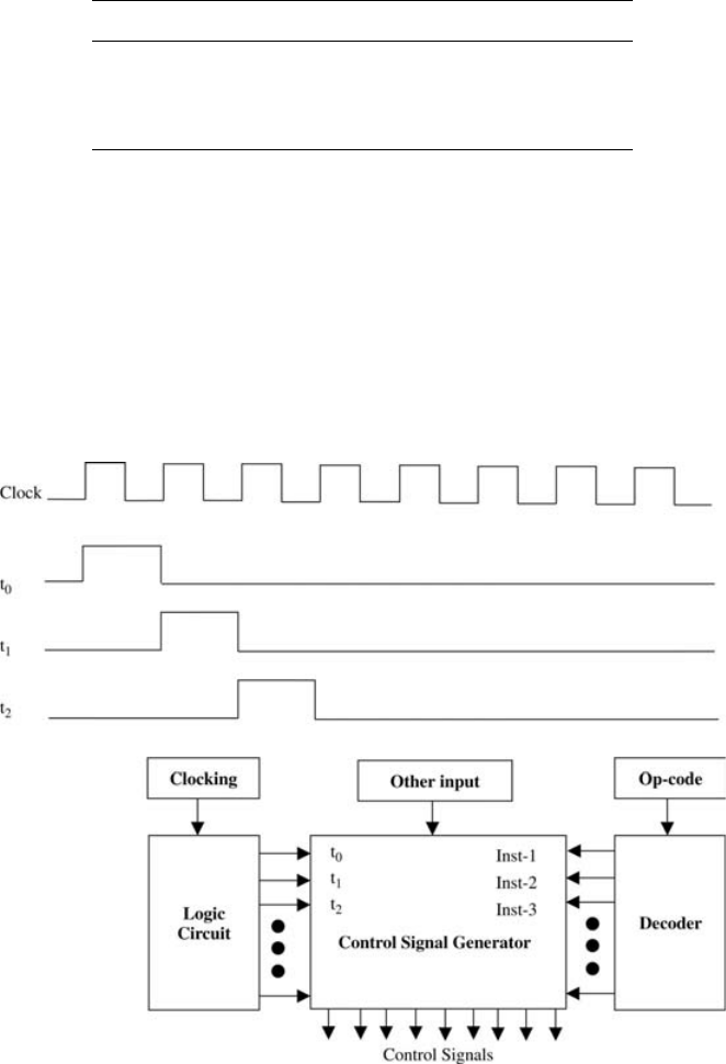
4. The contents of MDR (old value of the PC) are stored in memory.
The following table shows the sequence of events, where t
1
, t
2
, t
3
.
Step Micro-operation
t
1
MDR (PC)
t
2
MAR address1 (where to save old PC);
PC address2 (interrupt handling routine)
t
3
Mem[MAR] (MDR)
5.5. CONTROL UNIT
The control unit is the main component that directs the system operations by sending
control signals to the datapath. These signals control the flow of data within the CPU
and between the CPU and external units such as memory and I/O. Control buses
generally carry signals between the control unit and other computer components
in a clock-driven manner. The system clock produces a cont inuous sequence of
pulses in a specified duration and frequency. A sequence of steps t
0
, t
1
, t
2
, ...,
Figure 5.7 Timing of control signals
5.5. CONTROL UNIT 95

(t
0
, t
1
, t
2
,
...
) are used to execute a certain instruction. The op-code field of a
fetched instruction is decoded to provide the control signal generator with infor-
mation about the instru ction to be executed. Step information generated by a
logic circui t module is used with other inputs to generate control signals . The
signal generator can be specified simply by a set of Boolean equations for its
output in terms of its inputs. Figure 5.7 shows a bloc k diagram that describes how
timing is used in generating control signals.
There are mainly two different types of control units: microprogrammed and
hardwired. In microprogrammed control, the control signals associated with oper-
ations are stored in special memory units inaccessible by the programmer as control
words. A control word is a microinstruction that specifies one or more micro-
operations. A sequence of microinstructions is called a microprogram, which is
stored in a ROM or RAM called a control memory CM.
In hardwired control, fixed logic circuits that correspond directly to the Boolean
expressions are used to generate the control signals. Clearly hardwired control is
faster than microprogrammed control. However, hardwired control could be very
expensive and complicated for complex systems. Hardwired control is more econ-
omical for small control units. It should also be noted that microprogrammed control
could adapt easily to changes in the system design. We can easily add new instruc-
tions without changing hardware. Hardwired control will require a redesign of the
entire systems in the case of any change.
Example 1 Let us revisit the add operation in which we add the contents of source
registers R
1
, R
2
, and store the results in destination register R
0
. We have shown
earlier that this operation can be done in one step using the three-bus datapath
shown in Figure 5.5.
Let us try to examine the control sequence needed to accomplish this addition
at step t
0
. Suppose that the op-code field of the current instruction was decoded to
Inst-x type. First we need to select the source registers and the destination register,
then we select Add as the ALU function to be performed. The following table
shows the needed step and the control sequence.
Step Instruction type Micro-operation Control
t
0
Inst-x R
0
(R
1
) þ (R
2
) Select R
1
as source 1 on
out-bus1 (R
1
out-bus1)
Select R
2
as source 2 on
out-bus2 (R
2
out-bus2)
Select R
0
as destination
on in-bus (R
0
in-bus)
Select the ALU function
Add (Add)
Figure 5.8 shows the signals generated to execute Inst-x during time period t
0
.
The AND gate ensures that these signals will be issued when the op-code is decoded
into Inst-x and during time period t
0
. The signals (R
1
out-bus 1), (R
2
out-bus2),
96 PROCESSING UNIT DESIGN

(R
0
in-bus), and (Add) will select R
1
as a source on out-bus1, R
2
as a source on out-
bus2, R
0
as destination on in-bus, and select the ALUs add function, respectively.
Example 2 Let us repeat the operation in the previous example using the one-bus
datapath shown in Fig. 5.3. We have shown earlier that this operation can be carried
out in three steps using the one-bus datapath. Suppose that the op-code field of the
current instruction was decoded to Inst-x type. The following table shows the needed
steps and the control sequence.
Step Instruction type Micro-operation
t
0
Inst-x A (R
1
) Select R
1
as source (R
1
out)
Select A as destination (A in)
t
1
Inst-x B (R
2
) Select R
2
as source (R
2
out)
Select B as destination (B in)
t
2
Inst-x R
0
(A ) þ (B) Select the ALU function Add (Add)
Select R
0
as destination (R
0
in)
Figure 5.9 shows the signals generated to execute Inst-x during time periods t
0
,
t
1
, and t
2
. The AND gates ensure that the appropriate signals will be issued when the
op-code is decoded into Inst-x and during the appropriate time period. During t
0
, the
signals (R
1
out) and (A in) will be issued to move the contents of R
1
into A. Similarly
during t
1
, the signals (R
2
out) and (B in) will be issued to move the contents of R
2
into B. Finally, the signals (R
0
in) and (Add) will be issued during t
2
to add the con-
tents of A and B and move the results into R
0
.
5.5.1. Hardwired Implementation
In hardwired control, a direct implementation is accomplished using logic cir-
cuits. For each control line, one must find the Boolean expression in terms of the
input to the control signal generator as shown in Figure 5.7. Let us explain the
In-bus
Out-bus 1
ALU
Out-bus 2
t
0
Inst-x
R
0
R
1
R
2
R
0
in-bus
R
2
out-bus2
R
2
out-bus1
Add
Figure 5.8 Signals generated to execute Inst-x on three-bus datapath during time period t
0
5.5. CONTROL UNIT 97

implementation using a simple example. Assume that the instruction set of a
machine has the three instructions: Inst-x, Inst-y, and Inst-z; and A, B, C, D, E, F,
G, and H are control lines. The following table shows the control lines that
should be activated for the three instructions at the three steps t
0
, t
1
, and t
2
.
Step Inst-x Inst-y Inst-z
t
0
D, B, E F, H, G E, H
t
1
C, A, H G D, A, C
t
2
G, C B, C
The Boolean expressions for cont rol lines A, B, and C can be obtained as follows:
A ¼ Inst-x t
1
þ Inst-z t
1
¼ (Inst-x þ Inst-z) t
1
B ¼ Inst-x t
0
þ Inst-y t
2
C ¼ Inst-x t
1
þ Inst-x t
2
þ Inst-y t
2
þ Inst-z t
1
¼ (Inst-x þ Inst-z) t
1
þ (Inst-x þ Inst-y) t
2
Figure 5.10 shows the logic circuits for these control lines. Boolean expressions
for the rest of the control lines can be obtained in a similar way. Figure 5.11 shows
the state diagram in the execution cycle of these instructions.
5.5.2. Microprogrammed Control Unit
The idea of microprogrammed control units was introduced by M. V. Wilkes in the
early 1950s. Microprogramming was motivated by the desi re to reduce the complex-
ities involved with hardwired control. As we studied earlier, an instruction is
Figure 5.9 Signals generated to execute Inst-x on one-bus datapath during time period t
0
, t
1
, t
2
98 PROCESSING UNIT DESIGN

Inst-x
Inst-z
Inst-x
Inst-y
Inst-y
t
2
t
2
Inst-x
t
0
t
1
A
C
B
Figure 5.10 Logic circuits for control lines A, B, and C
Fetch the next
instruction
Decode
D, B, E
C, A, H
G, C
F, H, G
G
B, C
E, H
D, A, C
t
0
t
1
t
2
t
0
t
1
t
2
t
0
t
1
Inst-x
Inst-zInst-y
Figure 5.11 Instruction execution state diagram
5.5. CONTROL UNIT
99

implemented using a set of micro-operations. Associated with each micro-operation
is a set of control lines that must be activated to carry out the corresponding micro-
operation. The idea of microprogrammed control is to store the control signals
associated with the implementation of a certain instruction as a microprogram in
a special memory called a control memory (CM). A microprogram consists of a
sequence of microinstructions. A micro instruction is a vector of bits, where each
bit is a control signal, condition code, or the address of the next microinstruction.
Microinstructions are fetched from CM the same way program instructions are
fetched from main memory (Fig. 5.12).
When an instruction is fetched from memory, the op-code field of the instruc-
tion will determine which microprogram is to be executed. In other words, the
op-code is mapped to a microinstruction address in the control memory. The
microinstruction processor uses that address to fetch the first microinstruction in
the microprogram. After fetching each microinstruction, the appropriate control
lines will be enabl ed. Every control line that corresponds to a “1” bit should be
turned on. Every control line that corresponds to a “0” bit should be left off.
After completing the execution of one microinstruction, a new microinstruction
will be fetched and executed. If the condition code bits indicate that a branch
must be taken, the next microinstruction is specified in the address bits of the cur-
rent microinstruction. Otherwise, the next microinstruction in the sequence will be
fetched and executed.
The length of a microinstruction is determined based on the number of micro-
operations specified in the microinstructions, the way the control bits will be
interpreted, and the way the address of the next microinstruction is obtained. A
microinstruction may specify one or more micro-operations that will be activated
simultaneously. The length of the microinstruction will increase as the number of
parallel micro-operations per microinstruction increases. Furthermore, when each
control bit in the microinstruction corresponds to exactly one control line, the
length of microinstruction could get bigger. The length of a microinstru ction
could be reduced if control lines are coded in specific fields in the microinstruction.
Decoders will be needed to map each field into the individual control lines. Clearly ,
using the decoders will reduce the number of control lines that can be activated sim-
ultaneously. There is a tradeoff between the length of the microinstructions and the
amount of parallelism. It is important that we reduce the length of microinstructions
to reduce the cost and access time of the control memory. It may also be desirable
that more micro-operations be performed in parallel and more control lines can be
activated simultaneously.
External
input
Control
Control Address
Control data
Register
Sequencer
Control
Memory
Figure 5.12 Fetching microinstructions (control words)
100
PROCESSING UNIT DESIGN

Horizontal Versus Vertical Microinstructions Microinstructions can be
classified as horizontal or vertical. Individual bits in horizontal microinstructions
correspond to individual control lines. Horizontal microinstructions are long and
allow maximum parallelism since each bit controls a single control line. In
vertical microinstructions, control lines are coded into specific fields within a
microinstruction. Decoders are needed to map a field of k bits to 2
k
possible com-
binations of control lines. For example, a 3-bit field in a microinstruction could be
used to specify any one of eight possible lines. Because of the encoding, vertical
microinstructions are much shorter than horizontal ones. Control lines encoded
in the same field cannot be activated simultaneously. Therefore, vertical micro-
instructions allow only limit ed parallelism. It should be noted that no decoding
is needed in horizontal microinstructions while decoding is necessary in the
vertical case.
Example 3 Consider the three-bus datapath shown in Figure 5.5. In addition to
the PC, IR, MAR, and MDR, assume that there are 16 general-purpose registers
numbered R
0
–R
15
. Also, assume that the ALU supports eight functions (add, sub-
tract, multiply, divide, AND, OR, shift left, and shift right). Consider the add oper-
ation Add R
1
, R
2
, R
0
, which adds the contents of source registers R
1
, R
2
, and store
the results in destination register R
0
. In this example, we will study the format of the
microinstruction under horizont al organization.
We will use horizontal microinstructions, in which there is a control bit for
each control line. The format of the microinstruction should have control bits for
the following:
.
ALU operations
.
Registers that output to out-bus1 (source 1)
.
Registers that output to out-bus2 (source 2)
.
Registers that input from in-bus (destination)
.
Other operations that are not shown here
The following table shows the number of bits needed for ALU, Source 1,
Source 2, and destination:
Purpose Number of bits Explanations
ALU 8 bits 8 functions
Source 1 20 bits 16 general-purpose registers þ 4 special-
purpose registers
Source 2 16 bits 16 general-purpose registers
Destination 20 bits 16 general-purpose registers þ 4 special-
purpose registers
Figure 5.13 is the microinstruction for Add R
1
, R
2
, R
0
on the three-bus datapath.
5.5. CONTROL UNIT 101

Example 4 In this example, we will use vertical microinstructions, in which
decoders will be needed. We will use a three-bus datapath as shown in Figure 5.5.
Assume that there are 16 general-purpose registers and that the ALU supports eight
functions. The following tables show the encoding for ALU functions, registers
connected to out-bus 1 (Source 1), registers connected to out-bus 2 (Source 2),
and registers connected to in-bus (Destination).
Purpose Number of bits Explanations
ALU 4 bits 8 functions þ none
Source 1 5 bits 16 general-purpose registers þ 4 special-purpose
registers þ none
Source 2 5 bits 16 general-purpose registers þ none
Destination 5 bits 16 general-purpose registers þ 4 special-purpose
registers þ none
Encoding ALU function
0000 None (ALU will connect out-bus1 to in-bus)
0001 Add
0010 Subtract
0011 Multiple
0100 Divide
0101 AND
0110 OR
0111 Shift left
1000 Shift right
Encoding Source 1 Destination Encoding Source 2
00000 R
0
R
0
00000 R
0
00001 R
1
R
1
00001 R
1
00010 R
2
R
2
00010 R
2
00011 R
3
R
3
00011 R
3
00100 R
4
R
4
00100 R
4
00101 R
5
R
5
00101 R
5
00110 R
6
R
6
00110 R
6
00111 R
7
R
7
00111 R
7
01000 R
8
R
8
01000 R
8
01001 R
9
R
9
01001 R
9
01010 R
10
R
10
01010 R
10
Figure 5.13 Microinstruction for Add R
1
, R
2
, R
0
102 PROCESSING UNIT DESIGN

Encoding Source 1 Destination Encoding Source 2
01011 R
11
R
11
01011 R
11
01100 R
12
R
12
01100 R
12
01101 R
13
R
13
01101 R
13
01110 R
14
R
14
01110 R
14
01111 R
15
R
15
01111 R
15
10000 PC PC 10000 None
10001 IR IR
10010 MAR MAR
10011 MDR MDR
10100 NONE NONE
Figure 5.14 is the microinstruction for Add R
1
, R
2
, R
0
using the three-bus data-
path under vertical organization:
Example 5 Using the same encoding of Example 4, let us find vertical microin-
structions used in fetching an instruction.
MAR PC First, we need to select PC as source 1 by using “10000” for source 1
field. Similarly, we select MAR as our destination by using “10010” in the destina-
tion field. We also need to use “0000” for the ALU field, which will be decoded to
“NONE”. As shown in the ALU encoding table (Example 4), “NONE” means that
out-bus1 will be connected to in-bus. The field source 2 will be set to “10000”,
which means none of the registers will be select ed. The microinstruction is shown
in Figure 5.15.
Memory Read and Write Memory operations can easily be accommodated by
adding 1 bit for read and another for write. The two microinstructions in
Figure 5.16 perform memory read and write, respectively.
Fetch Fetching an instruction can be done using the three microinstructions of
Figure 5.17.
The first and second microinstructions have been shown above. The third microin-
struction moves the contents of the MDR to IR (IR MDR). MDR is selected as
source 1 by using “10011” for source 1 field. Similarly, IR is selected as the destina-
tion by using “10001” in the destination field. We also need to use “0000” (“NONE”)
Figure 5.14 Microinstruction for Add R
1
, R
2
, R
0
Figure 5.15 Microinstruction for MAR PC
5.5. CONTROL UNIT 103

in the ALU field, which means that out-bus1 will be connected to in-bus. The field
source 2 will be set to “10000”, which means none of the registers will be selected.
5.6. SUMMARY
The CPU is the part of a computer that interprets and carries out the instructions con-
tained in the programs we write. The CPU’s main components are the register file,
ALU, and the control unit. The register file contains general-purpose and special reg-
isters. General-purpose registers may be used to hold operands and intermediate results.
The special registers may be used for memory access, sequencing, status information,
or to hold the fetched instruction during decoding and execution. Arithmetic and logi-
cal operations are performed in the ALU. Internal to the CPU, data may move from one
register to another or between registers and ALU. Data may also move between the
CPU and external components such as memory and I/O. The control unit is the com-
ponent that controls the state of the instruction cycle. As long as there are instructions to
execute, the next instruction is fetched from main memory. The instruction is executed
based on the operation specified in the op-code field of the instruction. The control unit
generates signals that control the flow of data within the CPU and between the CPU and
external units such as memory and I/O. The control unit can be implemented using
hardwired or microprogramming techniques.
EXERCISES
1. How many instruction bits are required to specify the following:
(a) Two operand registers and one result register in a machine that has 64
general-purpose registers?
Figure 5.16 Microinstructions for memory read and write
Figure 5.17 Microinstructions for fetching an instruction
104
PROCESSING UNIT DESIGN

(b) Three memory addresses in a machine with 64 KB of main memory?
2. Show the micro-operations of the load, store, and jump instructions using:
(a) One-bus system
(b) Two-bus system
(c) Three-bus system
3. Add control signals to all the tables in Section 5.4.
4. Data movement within the CPU can be performed in several different
ways. Contrast the following methods in terms of their advantages and
disadvantages:
(a) Dedicated connections
(b) One-bus datapat h
(c) Two-bus datapath
(d) Three-bus datapath
5. Find a method of encoding the microinstructions described by the following
table so that the minimum number of control bits is used and all inherent
parallelism among the microoperations is pres erved.
Microinstruction Control signals activated
I
1
a, b, c, d, e
I
2
a, d, f, g
I
3
b, h
I
4
c
I
5
c, e, g, i
I
6
a, h, j
6. Suppose that the instruction set of a machine has three instructions: Inst-1,
Inst-2, and Inst-3; and A, B, C, D, E, F, G, and H are the control lines.
The following table shows the control lines that should be activated for
the three instructions at the three steps T0, T1, and T2.
Step Inst-1 Inst-2 Inst-3
T0 D, B, E F, H, G E, H
T1 C, A, H G D, A, C
T2 G, C B, C
(a) Hardwired approach:
(i) Write Boolean expressions for all the control lines A–G.
(ii) Draw the logic circuit for each control line.
(b) Microprogramming approach:
(i) Assuming a horizontal representation, write down the micropro-
gram for instructions Inst-1. Indicate the microinstruction size.
EXERCISES 105
(ii) If we allow both horizontal and vertical represe ntation, what would
be the best grouping? What is the microinstruction size? Write the
microprogram of Inst-1.
7. A certain processor has a microinstruction format containing 10 separate
control fields C
0
: C
9
. Each C
i
can activate any one of n
i
distinct control
lines, where n
i
is specified as follows:
i: 012 3 4 5 6789
n
i
:4431191671822
(a) What is the minimum number of control bits needed to represent the 10
control fields?
(b) What is the maximum number of control bits needed if a purely horizon-
tal format is used for all control information?
8. What are the main differences between the following pairs?
(a) Vertical and horizontal microinstructions
(b) Microprogramming and hardwired control
9. Using the single-bus architecture, generate the necessary control signals,
in the proper order (with minimu m number of micro-instructions), for
conditional branch instruction.
10. Write a micro-program for the fetch instruction using the one-bus datapath
and the two-bus datapath.
REFERENCES AND FURTHER READING
R. J. Baron and L. Higbie, Computer Architecture, Addison Wesley, Canada, 1992.
M. J. Flynn, Computer Architecture, Jones and Barlett, MA, USA, 1995.
J. P. Hayes, Computer Architecture and Organization, McGraw-Hill, New York, 1998.
J. Hennessy and D. Patterson, Computer Architecture: A Quantitative Approach, Morgan
Kaufmann, San Francisco, CA, 2003.
V. P. Heuring and H. F. Jordan, Computer Systems Design and Architecture, Addison Wesley,
NJ, 1997.
M. Murdocca and V. Heuring, Principles of Computer Architecture, Prentice Hall, NJ,
USA, 2000.
D. Patterson and J. Hennessy, Computer Organization and Design, Morgan Kaufmann,
San Mateo, CA, 1998.
W. Stallings, Computer Organization and Architecture: Designing for Performance, NJ, 1996.
A. S. Tanenbaum, Structured Computer Organization, Prentice Hall, NJ, USA, 1999.
106
PROCESSING UNIT DESIGN

&
CHAPTER 6
Memory System Design I
In this chapter, we study the computer memory system. It was stated in Chapter 3
that without a memory no information can be stored or retrieved in a computer. It
is interesting to observe that as early as 1946 it was recognized by Burks, Goldstine,
and Von Neumann that a computer memory has to be organ ized in a hierarchy. In
such a hierarchy, larger and slower memorie s are used to supplement smaller and
faster ones. This observation has since then proven essential in constructing a com-
puter memory. If we put aside the set of CPU registers (as the first level for storing
and retrieving information inside the CPU, see Chapter 5), then a typical memory
hierarchy starts with a small, expensive, and relatively fast unit, called the cache.
The cache is followed in the hierarchy by a larger, less expensive, and relatively
slow main memory unit. Cache and main memory are built using solid-state semi-
conductor material. They are followed in the hierarchy by far larger, less expensive,
and much slower magnetic memories that consist typically of the (hard) disk and the
tape. Our deliberation in this chapter starts by discussing the characteristics and fac-
tors influencing the success of a memory hierarchy of a computer. We then direct our
attention to the design and analysis of cache memory. Discussion on the (main)
memory unit is conducted in Chapter 7. Also discussed in Chapter 7 are the
issues related to virtual memory design. A brief coverage of the different read-
only memory (ROM) implementations is also provided in Chapter 7.
6.1. BASIC CONCEPTS
In this section, we introduce a number of fundamental concepts that relate to the
memory hierarchy of a computer.
6.1.1. Memory Hierarchy
As mentioned above, a typical memory hierarchy starts with a small, expensive, and
relatively fast unit, called the cache, followed by a larger, less expensive, and rela-
tively slow main memory unit. Cache and main memory are built using solid-state
107
Fundamentals of Computer Organization and Architecture, by M. Abd-El-Barr and H. El-Rewini
ISBN 0-471-46741-3 Copyright # 2005 John Wiley & Sons, Inc.

semiconductor material (typically CMOS transistors). It is customary to call the fast
memory level the primary memory. The solid-state memory is followed by larger, less
expensive, and far slower magnetic memories that consist typically of the (hard) disk
and the tape. It is customary to call the disk the secondary memory, while the tape is con-
ventionally called the tertiary memory. The objective behind designing a memory hier-
archy is to have a memory system that performs as if it consists entirely of the fastest unit
and whose cost is dominated by the cost of the slowest unit.
The memory hierarchy can be characterized by a number of parameters. Among these
parameters are the access type, capacity, cycle time, latency, bandwidth,andcost.The
term access refers to the action that physically takes place during a read or write oper-
ation. The capacity of a memory level is usually measured in bytes. The cycle time is
defined as the time elapsed from the start of a read operation to the start of a subsequent
read. The latency is defined as the time interval between the request for information and
the access to the first bit of that information. The bandwidth provides a measure of the
number of bits per second that can be accessed. The cost of a memory level is usually
specified as dollars per megabytes. Figure 6.1 depicts a typical memory hierarchy.
Table 6.1 provides typical values of the memory hierarchy parameters.
The term random access refers to the fact that any access to any memory location
takes the same fixed amount of time regardless of the actual memory location and/or
the sequence of accesses that takes place. For example, if a write operation to
memory location 100 takes 15 ns and if this operation is followed by a read oper-
ation to memory location 3000, then the latter operation will also take 15 ns. This
is to be compared to sequential access in which if access to location 100 takes
500 ns, and if a consecutive access to location 101 takes 505 ns, then it is expected
that an access to location 300 may take 1500 ns. This is because the memory has to
cycle through locations 100 to 300, with each location requiring 5 ns.
The effectiveness of a memory hierarchy depends on the principle of moving
information into the fast memory infrequently and accessing it many times before
replacing it with new information. This principle is possible due to a phenomenon
called locality of reference; that is, within a given period of time, programs tend
to reference a relatively confined area of memory repeatedly. There exis t two
forms of locality: spatial and temporal locality. Spatial locality refers to the
CPU Registers
Cache
Latency
Main Memory
Bandwidth
Secondary Storage (Disk)
Speed
Cost per bit
TertiaryStorage (Tape)
Capacity (megabytes)
Figure 6.1 Typical memory hierarchy
108
MEMORY SYSTEM DESIGN I

phenomenon that when a given address has been referenced, it is most likely that
addresses near it will be referenced within a short period of time, for example, consecu-
tive instructions in a straightline program. Temporal locality, on the other hand, refers
to the phenomenon that once a particular memory item has been referenced, it is most
likely that it will be referenced next, for example, an instruction in a program loop.
The sequence of events that takes place when the processor makes a request for an
item is as follows. First, the item is sought in the first memory level of the memory
hierarchy. The probability of finding the requested item in the first level is called
the hit ratio, h
1
. The probability of not finding (missing) the requested item in the
first level of the memory hierarchy is called the miss ratio,(12 h
1
). When the
requested item causes a “miss,” it is sought in the next subsequent memory level.
The probability of finding the requested item in the second memory level, the hit
ratio of the second level, is h
2
. The miss ratio of the second memory level is
(1 h
2
). The process is repeated until the item is found. Upon finding the requested
item, it is brought and sent to the processor. In a memory hierarchy that consists of
three levels, the average memory access time can be expressed as follows:
t
av
¼ h
1
t
1
þ (1 h
1
)½t
1
þ h
2
t
2
þ (1 h
2
)(t
2
þ t
3
)
¼ t
1
þ (1 h
1
)½t
2
þ (1 h
2
)t
3
The average access time of a memory level is defined as the time required to access
onewordinthatlevel.Inthisequation,t
1
, t
2
, t
3
represent, respectively, the access
times of the three levels.
6.2. CACHE MEMORY
Cache memory owes its introduction to Wilkes back in 1965. At that time, Wilkes
distinguished between two types of main memory: The conventional and the slave
memory. In Wilkes terminology, a slave memory is a second level of unconventional
high-speed memory, which nowadays corresponds to what is called cache memory
(the term cache means a safe place for hiding or storing things).
The idea behind using a cache as the first level of the memory hierarchy is to keep
the information expected to be used more frequently by the CPU in the cache
TABLE 6.1 Memory Hierarchy Parameters
Access type Capacity Latency Bandwidth Cost/MB
CPU registers Random 64– 1024 bytes 1–10 ns System clock
rate
High
Cache memory Random 8– 512 KB 15– 20 ns 10–20 MB/s $500
Main memory Random 16–512 MB 30–50 ns 1 –2 MB/s $20– 50
Disk memory Direct 1 –20 GB 10–30 ms 1 –2 MB/s $0.25
Tape memory Sequential 1–20 TB 30–10,000 ms 1–2 MB/s $0.025
6.2. CACHE MEMORY 109

(a small high-speed memory that is near the CPU). The end result is that at any given
time some active portion of the main memory is duplicated in the cache. Therefore,
when the processor makes a request for a memory reference, the request is first
sought in the cache. If the request corresponds to an element that is currently resid-
ing in the cache, we call that a cache hit. On the other hand, if the request corre-
sponds to an element that is not currently in the cache, we call that a cache miss.
A cache hit ratio, h
c
, is defined as the probability of finding the requested element
in the cache. A cache miss ratio (1 h
c
) is defined as the probability of not finding
the requested element in the cache.
In the case that the requested element is not found in the cache, then it has to be
brought from a subsequent memory level in the memory hierarchy. Assuming that
the element exists in the next memor y level, that is, the main memory, then it has
to be brought and placed in the cache. In expectation that the next requested element
will be residing in the neighboring locality of the current requested element (spatial
locality), then upon a cache miss what is actually brought to the main memory is a
block of elements that contains the requested element. The advantage of transferring
a block from the main memory to the cache will be most visible if it could be poss-
ible to transfer such a block using one main memory access time. Such a possibility
could be achieved by increasing the rate at which information can be transferred
between the main memory and the cache. One possible technique that is used to
increase the bandwidth is memory interleaving. To achieve best results, we can
assume that the block brought from the main memory to the cache, upon a cache
miss, consists of elements that are stored in different memory modules, that is,
whereby consecutive memory addresses are stored in successive memory modules.
Figure 6.2 illustrates the simple case of a main memory consisting of eight memory
modules. It is assumed in this case that the block consists of 8 bytes.
Having introduced the basic idea leading to the use of a cache memory, we would
like to assess the impact of temporal and spatial locality on the performance of
the memory hierarchy. In order to make such an assessment, we will limit our
M
7
M
6
M
5
M
4
M
3
M
2
M
1
M
0
Byte
Main memory
Block
Cache
Figure 6.2 Memory interleaving using eight modules
110
MEMORY SYSTEM DESIGN I

deliberation to the simple case of a hierarchy consisting only of two levels, that is,
the cache and the main memory. We assume that the main memory access time is t
m
and the cache access time is t
c
. We will measure the impact of locality in terms of the
average access time, defined as the average time required to access an element (a
word) requested by the processor in such a two-level hierarchy.
6.2.1. Impact of Temporal Locality
In this case, we assume that instructions in program loops, which are executed many
times, for example, n times, once loaded into the cache, are used more than once
before they are replaced by new instructions. The average access time, t
av
,isgivenby
t
av
¼
nt
c
þ t
m
n
¼ t
c
þ
t
m
n
In deriving the above expression, it was assumed that the requested memory element
has created a cache miss, thus leading to the transfer of a main memory block in time
t
m
. Following that, n accesses were made to the same requested element, each taking
t
c
. The above expression reveals that as the number of repeated accesses, n,increases,
the average access time decreases, a desirable feature of the memory hierarchy.
6.2.2. Impact of Spatial Locality
In this case, it is assumed that the size of the block transferred from the main
memory to the cache, upon a cache miss, is m elements. We also assume that due
to spatial locality, all m elements were requested, o ne at a time, by the processor.
Based on these assumptions, the average access time, t
av
, is given by
t
av
¼
mt
c
þ t
m
m
¼ t
c
þ
t
m
m
In deriving the above expression, it was assumed that the requested memory element
has created a cache miss, thus leading to the transfer of a main memory block, con-
sisting of m elements, in time t
m
. Following that, m accesses, each for one of the
elements constituting the block, were made. The above expression reveals that as
the number of elements in a block, m, increases, the average access time decreases,
a desirable feature of the memory hierarchy.
6.2.3. Impact of Combined Temporal and Spatial Locality
In thi s case, we assume that the element requested by the processor created a cache
miss leading to the transfer of a block, consisting of m elements, to the cache (that
take t
m
). Now, due to spatial locality, all m elements constituting a block were
requested, one at a time, by the processor (requiring mt
c
). Following that, the orig-
inally requested element was accessed (n 2 1) times (temporal locality), that is, a
6.2. CACHE MEMORY 111

total of n times access to that element. Based on these assumptions, the average
access time, t
av
, is given by
t
av
¼
mt
c
þ t
m
m
þ (n 1)t
c
n
¼
t
c
þ
t
m
m
þ (n 1)t
c
n
¼
t
m
nm
þ t
c
A further simplifying assumption to the above expression is to assume that t
m
¼ mt
c
.
In this case the above expression will simplify to
t
av
¼
mt
c
nm
þ t
c
¼ t
c
þ
t
c
n
¼
n þ 1
n
t
c
The above expression reveals that as the number of repeated accesses n increases, the
average access time will approach t
c
. This is a significant performance improvement.
It should be clear from the above discussion that as more requests for items that
do not exist in the cache (cache miss) occur, more blocks would have to be brought
to the cache. This should raise two basic questions: Where to place an incoming
main memory block in the cache? And in the case where the cache is totally
filled, which cache block shoul d the incoming main memory block replace? Place-
ment of incoming blocks and replacement of existing blocks are performed accord-
ing to specific protocols (algorithms). These protocols are strongly related to the
internal organization of the cache. Cache internal organization is discussed in the
following subsections. However, before discussing cache organization, we first
introduce the cache-mapping function.
6.2.4. Cache-Mapping Function
Without loss of generality, we present cache-mapping function taking into consider-
ation the interface between two successive levels in the memory hierarchy: primary
level and secondary level. If the focus is on the interface between the cache and main
memory, then the cache represents the primary level, while the main memory rep-
resents the secondary level. The same principles apply to the interface between any
two memory levels in the hierarchy. In the following discussion, we focus our atten-
tion to the interface between the cache and the main memory.
It should be noted that a request for accessing a memory ele ment is made by the
processor through issuing the address of the requested element. The address issued
by the processor may correspond to that of an element that exists currently in the
cache (cache hit); otherwise, it may correspond to an element that is currently resid-
ing in the main memory. Therefore, address translation has to be made in order to
determine the whereabouts of the requested element. This is one of the functions
performed by the memory management unit (MMU). A schematic of the address
mapping function is shown in Figure 6.3.
In this figure, the system address represents the address issued by the processor
for the requested element. This address is used by an address translation function
inside the MMU. If address translation reveals that the issued address corresponds
to an element currently residing in the cache , then the eleme nt will be made
112 MEMORY SYSTEM DESIGN I

available to the processor. If, on the other hand, the element is not currently in the
cache, then it will be brought (as part of a block) from the main memory and placed
in the cache and the element requested is made available to the processor.
6.2.5. Cache Memory Organization
There are three main different organ ization techniques used for cache memory. The
three techniques are discussed below. These techniques differ in two main aspects:
1. The criterion used to place, in the cache, an incoming block from the main
memory.
2. The criterion used to replace a cache block by an incoming block (on cache full).
Direct Mapping This is the simplest among the three techniques. Its simplicity
stems from the fact that it places an incoming main memory block into a specific
fixed cache block location. The placement is done based on a fixed relation between
the incoming block number, i, the cache block number, j, and the number of cache
blocks, N:
j ¼ i mod N
Example 1 Consider, for example, the case of a main memory consisting of 4K
blocks, a cache memory consisting of 128 blocks, and a block size of 16 words.
Figure 6.4 shows the division of the main memory and the cache according to the
direct-mapped cache techniq ue.
As the figure shows, there are a total of 32 main memory blocks that map to
a given cache block. For example, main memory bloc ks 0, 128, 256, 384, ... ,
3968 map to cache bloc k 0. We therefore call the direct-mapping technique a
The requested element
Memory Management
Unit (MMU)
Secondary
Level
Block
Primary Level
Address in
Primary Memory
Miss
System
Address
Translation
Function
Hit
Figure 6.3 Address mapping operation
6.2. CACHE MEMORY 113

many-to-one mapping technique. The main advantage of the direct-mapping tech-
nique is its simplicity in determining where to place an incoming main memor y
block in the cache. Its main disadvantage is the inefficient use of the cache. This
is because according to this technique, a number of main memory blocks may com-
pete for a given cache block even if there exist other empty cache blocks. This dis-
advantage should lead to achieving a low cache hit ratio.
According to the direct-mapping technique the MMU interprets the address issued
by the processor by dividing the address into three fields as shown in Figure 6.5. The
lengths, in bits, of each of the fields in Figure 6.5 are:
1. Word field ¼ log
2
B, where B is the size of the block in words.
2. Block field ¼ log
2
N, where N is the size of the cache in blocks.
3. Tag field ¼ log
2
(M/N), where M is the size of the main memory in blocks.
4. The number of bits in the main memory address ¼ log
2
(B M)
It should be noted that the total number of bits as computed by the first three
equations should add up to the length of the main memory address. This can be
used as a check for the correctness of your computation.
Example 2 Compute the above four parameters for Example 1.
Word field ¼ log
2
B ¼ log
2
16 ¼ log
2
2
4
¼ 4 bits
Block field ¼ log
2
N ¼ log
2
128 ¼ log
2
2
7
¼ 7 bits
Tag field ¼ log
2
(M/N) ¼ log
2
(2
2
2
10
/2
7
) ¼ 5 bits
The number of bits in the main memory address ¼ log
2
(B M) ¼ log
2
(2
4
2
12
) ¼ 16 bits.
3
Tag
1
0
31
384
Cache
129
0
1
2
126
127
4095
Main Memory
0
1
2
128
129
130
256
257
258
384
385
386
3968
127 255 383 4095
0123 31
Figure 6.4 Mapping main memory blocks to cache blocks
Figure 6.5 Direct-mapped address fields
114
MEMORY SYSTEM DESIGN I

Having shown the division of the main memory addre ss, we can now proceed to
explain the prot ocol used by the MMU to satisfy a request made by the processor for
accessing a given element. We illustrate the protocol using the parameters given in
the example presented above (Fig. 6.6).
The steps of the protocol are:
1. Use the Block field to determine the cache block that should contain the element
requested by the processor. The Block field is used directly to determine the
cache block sought, hence the name of the technique: direct-mapping.
2. Check the corresponding Tag memory to see whether there is a match between
its content and that of the Tag field. A match between the two indicates that the
targeted cache block determined in step 1 is currently holding the main
memory element requested by the processor, that is, a cache hit.
3. Among the elements contained in the cache block, the targeted element can be
selected using the Word field.
4. If in step 2, no match is found, then this indicates a cache miss. Therefore, the
required block has to be brought from the main memory, deposited in the cache,
and the targeted element is made available to the processor. The cache Tag
memory and the cache block memory have to be updated accordingly.
Figure 6.6 Direct-mapped address translation
6.2. CACHE MEMORY 115
The direct-mapping technique answers not only the placement of the incoming main
memory block in the cache question, but it also answers the replacement question.
Upon encountering a totally filled cache while a new main memory block has to be
brought, the replacement is trivial and determined by the equation j ¼ i mod N.
The main advantages of the direct-mapping technique is its simplicity measured
in terms of the direct determination of the cache block; no search is needed. It is also
simple in terms of the replacement mechanism. The main disadvant age of the tech-
nique is its expected poor utilization of the cache memory. This is represented in
terms of the possibility of targeting a given cache block, which requires frequent
replacement of blocks while the rest of the cache is not used. Consider, for example,
the sequence of requests made by the processor for elements held in the main
memory blocks 1, 33, 65, 97, 129, and 161. Consider also that the cache size is
32 blocks. It is clear that all the above blocks map to cache block number 1. There-
fore, thes e blocks will compete for that same cache block despite the fact that the
remaining 31 cache blocks are not used.
The expected poor utilization of the cache by the direct mapping technique is
mainly due to the restriction on the placement of the incoming main memory
blocks in the cache (the many-to-one property). If such a restriction is relaxed,
that is, if we make it possible for an incoming main memory block to be placed
in any empty (available) cache block, then the resulting technique would be so flex-
ible that efficient utilization of the cache would be possible. Such a flexible tech-
nique, called the Associative Mapping technique, is explained next.
Fully Associative Mapping According to this technique, an incoming main
memory block can be placed in any available cache block. Therefore, the address
issued by the processor need only have two fields. These are the Tag and Word
fields. The first uniquely identifies the block while residing in the cache. The
second field identifies the element within the block that is requested by the pro-
cessor. The MMU interprets the address issued by the processor by dividing it
into two fields as shown in Figure 6.7. The length, in bits, of each of the fields in
Figure 6.7 are given by:
1. Word field ¼ log
2
B, where B is the size of the block in words
2. Tag field ¼ log
2
M, where M is the size of the main memory in blocks
3. The number of bits in the main memory address ¼ log
2
(B M)
It should be noted that the total number of bits as computed by the first two equations
should add up to the length of the main memory address. This can be used as a check
for the correctness of your computation.
Figure 6.7 Associative-mapped address fields
116
MEMORY SYSTEM DESIGN I

Example 3 Compute the above three parameters for a memory system having the
following speci fication: size of the main memory is 4K blocks, size of the cache is
128 blocks, and the block size is 16 words. Assume that the system uses associative
mapping.
Word field ¼ log
2
B ¼ log
2
16 ¼ log
2
2
4
¼ 4 bits
Tag field ¼ log
2
M ¼ log
2
2
7
2
10
¼ 12 bits
The number of bits in the main memory address ¼ log
2
(B M) ¼ log
2
(2
4
2
12
) ¼ 16 bits.
Having shown the division of the main memory addre ss, we can now proceed to
explain the prot ocol used by the MMU to satisfy a request made by the processor for
accessing a given element. We illustrate the protocol using the parameters given in
the example presented above (see Fig. 6.8). The steps of the protocol are:
1. Use the Tag field to search in the Tag memory for a match with any of the tags
stored.
2. A match in the tag memory indicates that the corresponding targeted cache
block determined in step 1 is currently holding the main memory element
requested by the processor, that is, a cache hit.
Figure 6.8 Associative-mapped address translation
6.2. CACHE MEMORY 117
3. Among the elements contained in the cache block, the targeted element can be
selected using the Word field.
4. If in step 2, no match is found, then this indicates a cache miss. Therefore, the
required block has to be brought from the main memory, deposited in the first
available cache block, and the targeted element (word) is made available to
the processor. The cache Tag memory and the cache block memory have to
be updated accordingly.
It should be noted that the search made in step 1 above requires matching the tag
field of the address with each and every entry in the tag memory. Such a search, if
done sequentially, could lead to a long delay. Therefore, the tags are stored in an
associative (content addressable) memory. This allows the entire contents of the
tag memory to be searched in parallel (associatively), hence the name, associative
mapping.
It should be noted that, regardless of the cache organ ization used, a mechanism is
needed to ensure that any accessed cache block contains valid information. The val-
idity of the information in a cache block can be checked via the use of a single bit for
each cache block, called the valid bit. The valid bit of a cache block should be
updated in such a way that if valid bit ¼ 1, then the corresponding cache block car-
ries valid information; otherwise, the information in the cache block is invalid.
When a computer system is powered up, all valid bits are made equal to 0, indicating
that they carry invalid information. As blocks are brought to the cache, their statuses
are changed accordingly to indicate the validity of the information contained.
The main advantage of the associative-mapping technique is the efficient use of
the cache. This stems from the fact that there exists no restriction on where to place
incoming main memory blocks. Any unoccupied cache block can potentially be
used to receive those incoming main memory blocks. The main disadvantage of
the technique, however, is the hardware overhead required to perform the associat-
ive search conducted in order to find a match between the tag field and the tag
memory as discussed above.
A compromise between the simple but inefficient direct cache organization and
the involved but efficient associative cache organization can be achieved by con-
ducting the search over a limited set of cache blocks while kno wing ahead of
time where in the cache an incoming main memory block is to be placed. This is
the basis for the set-associative mapping technique explained next.
Set-Associative Mapping In the set-associative mapping technique, the cache
is divided into a number of sets. Each set consist s of a number of blocks. A given
main memory block maps to a specific cache set based on the equation
s ¼ i mod S, where S is the number of sets in the cache, i is the main memory
block number, and s is the specfic cache set to which block i maps. However, an
incoming block maps to any block in the assigned cache set. Therefore, the address
issued by the processor is divided into three distinct fields. Th ese are the Tag, Set,
and Word fields. The Set field is used to uniquely identify the specific cache set
118 MEMORY SYSTEM DESIGN I

that ideally should hold the targeted block. The Tag field uniquely identifies the tar-
geted block within the determined set. The Word field identifies the element (word)
within the block that is requested by the processor. According to the set-associative
mapping technique, the MMU interprets the address issued by the processor by
dividing it into three fields as shown in Figure 6.9. The length, in bits, of each of
the fields of Figure 6.9 is given by
1. Word field ¼ log
2
B, where B is the size of the block in words
2. Set field ¼ log
2
S, where S is the number of sets in the cache
3. Tag field ¼ log
2
(M/S), where M is the size of the main memory in blocks.
S ¼ N=B
s
, where N is the number of cache blocks and B
s
is the number of
blocks per set
4. The number of bit s in the main memory address ¼ log
2
(B M)
It should be noted that the total number of bits as computed by the first three
equations should add up to the length of the main memory address. This can be
used as a check for the correctness of your computation.
Example 4 Compute the above three parameters (Word, Se t, and Tag) for a
memory system having the following specification: size of the main memory is
4K blocks, size of the cache is 128 blocks, and the block size is 16 words.
Assume that the system uses set-associative mapping with four blocks per set.
S ¼
128
4
¼ 32 sets:
1. Word field ¼ log
2
B ¼ log
2
16 ¼ log
2
2
4
¼ 4 bits
2. Set field ¼ log
2
32 ¼ 5 bits
3. Tag field ¼ log
2
(4 2
10
/32) ¼ 7 bits
The number of bits in the main memory address ¼ log
2
(B M) ¼ log
2
(2
4
2
12
) ¼ 16 bits.
Having shown the division of the main memory addre ss, we can now proceed to
explain the prot ocol used by the MMU to satisfy a request made by the processor for
accessing a given element. We illustrate the protocol using the parameters given in
the example presented above (see Fig. 6.10). The steps of the protocol are:
1. Use the Set field (5 bits) to determine (directly) the specified set (1 of the
32 sets).
Figure 6.9 Set-associative-mapped address fields
6.2. CACHE MEMORY 119

2. Use the Tag field to find a match with any of the (four) blocks in the deter-
mined set. A match in the tag memory indicates that the specified set deter-
mined in step 1 is currently holding the targeted block, that is, a cache hit.
3. Among the 16 words (elements) contained in hit cache block, the requested
word is selected using a selector with the help of the Word field.
Tag
Cache
Block # 0
Main Memory Address
Tag Field
754
Set Field Word Field
031
Step #1
Step #2
Associative Search
Over the set
Block # 1
Block # 2
Block # 3
7 bits
Set 0
Set 1
Selector
Requested Word
Set i
Set 31
127
1 129
0 384
Figure 6.10 Set-associative-mapped address translation
120
MEMORY SYSTEM DESIGN I

4. If in step 2, no match is found, then this indicates a cache miss. Therefore,
the required block has to be brought from the main memory, deposited in
the specified set first, and the targeted element (word) is made available to
the processor. The cache Tag memory and the cache block memory have to
be updated accordingly.
It should be noted that the search made in step 2 above requires matching the tag
field of the address with each and every entry in the tag memory for the specified set.
Such a search is performed in parallel (associatively) over the set, hence the name,
set-associative mapping. The hardware overhead required to performing the associ-
ative search within a set in order to find a match between the tag field and the tag
memory is not as complex as that used in the case of the fully associative technique.
The set-associative-mapping technique is expected to produce a moderate cache
utilization efficiency, that is, not as efficient as the fully associative technique and
not as poor as the direct technique. However, the technique inherits the simplicity
of the direct mapping technique in terms of determining the target set.
An overall qualitative comparison among the three mapping techniques is shown
in Table 6.2. Owing to its moderate complexity and moderate cache utilization, the
set-associative techniq ue is used in the Intel Pentium line of processors.
The discussion above shows how the associative-mapping and the set-associative
techniques answer the question about the placement of the incoming main memory
block in the cache. The other important question that was posed at the beginning of
the discussion on cache memory is that of replacement. Specifically, upon encoun-
tering a totally filled cache while a new main memory block has to be brought, which
of the cache blocks should be selected for replacement? This is discussed below.
6.2.6. Replacement Techniques
A number of replacement techniques can be used. These include a randomly selected
block (random selection), the block that has been in the cache the longest ( first-in-
first-out, FIFO ), and the block that has been used the least while residing in the
cache (least recently used, LRU).
Let us assume that when a computer system is powered up, a random number
generator starts generating numbers between 0 and (N 2 1). As the name indicates,
TABLE 6.2 Qualitative Comparison Among Cache Mapping
Techniques
Mapping
technique Simplicity
Associative
tag search
Expected
cache
utilization
Replacement
technique
Direct Yes None Low Not needed
Associative No Involved High Yes
Set-associative Moderate Moderate Moderate Yes
6.2. CACHE MEMORY 121
random selection of a cache block for replacement is done based on the output of the
random number generator at the time of replacement. This technique is simple and
does not require much additional overhead. However, its main shortcoming is that it
does not take locality into consideration. Random techniques have been found effec-
tive enough such that they have been first used by Intel in its iAPX microprocessor
series.
The FIFO technique takes the time spent by a block in the cache as a measure for
replacement. The block that has been in the cache the longest is selected for replace-
ment regardless of the recent pattern of access to the block. This technique requires
keeping track of the lifetime of a cache block. Therefore, it is not as simple as the
random selection technique. Intuitively, the FIFO technique is reasonable to use
for straightline programs where locality of reference is not of concern.
According to the LRU replacement technique, the cache block that has been
recently used the least is selected for replacement. Among the three replacement
techniques, the LRU technique is the most effective. This is because the history
of block usage (as the criterion for replacement) is taken into consideration. The
LRU algorithm requires the use of a cache controller circuit that keeps track of refer-
ences to all blocks while residing in the cache. This can be achieved through a
number of possible implementations. Among these implementations is the use of
counters. In this case each cache block is assigned a counter. Upon a cache hit,
the counter of the correspo nding block is set to 0, all other counters having a smaller
value than the original value in the counter of the hit block are incremented by 1, and
all counters having a larger value are kept unchanged. Upon a cache miss, the block
whose counter is showing the maximum value is chosen for replacement, the counter
is set to 0, and all other counters are incremented by 1.
Having introduced the above three cache mapping technique, we offer the follow-
ing example, which illustrates the main observations made about the three techniques.
Example 5 Consider the case of a 48 two-dimensional array of numbers, A.
Assume that each number in the array occupies one word and that the array elements
are stored column-major order in the main memory from location 1000 to location
1031. The cache consists of eight blocks each consisting of just two words. Assume
also that whenever needed, LRU replacement policy is used. We would like to exam-
ine the changes in the cache if each of the above three mapping techniques is used as
the following sequence of requests for the array elements are made by the processor:
a
0,0
, a
0,1
, a
0,2
, a
0,3
, a
0,4
, a
0,5
, a
0,6
, a
0,7
a
1,0
, a
1,1
, a
1,2
, a
1,3
, a
1,4
, a
1,5
, a
1,6
, a
1,7
Solution The distribution of the array elements in the main memory is shown in
Figure 6.11. Shown also is the status of the cache before the above requests were made.
Direct Mapping Table 6.3 shows that there were 16 cache misses (not a single
cache hit) and that the number of replacements made is 12 (these are shown
122 MEMORY SYSTEM DESIGN I

tinted). It also shows that out of the available eight cache blocks, only four (0, 2, 4,
and 6) are used, while the remaining four are inactive all the time. This represents a
50% cache utilization.
Fully Ass ociative Mapping Table 6.4 shows that there were eight cache hits
(50% of the total number of requests) and that there were no replacements made.
It also shows a 100% cache utilization.
Set-Associative Mapping (With Two Blocks per Set) Table 6.5 shows that
there were 16 cache misses (not a single cache hit) and that the number of replace-
ments made is 12 (these are shown tinted). It also shows that of the available four
cache sets, only two sets are used, while the remaining two are inactive all the
time. This represents a 50% cache utilization.
Figure 6.11 Array elements in the main memory
6.2. CACHE MEMORY 123

6.2.7. Cache Write Policies
Having discussed the main issues related to cache mapping techniques and the repla-
cement policies, we would like to address a very important related issue, that is,
cache coherence. Coherence between a cache word and its copy in the main
memory should be maintained at all times, if at all possible. A number of policies
(techniques) are used in performing write operations to the main memory blocks
while residing in the cache. These policies determine the degree of coherence that
TABLE 6.3 Direct Mapping
Request
Cache
hit/miss
MM
block
number
(i)
Cache
block
number
(j)
Cache status
BL0 BL1 BL2 BL3 BL4 BL5 BL6 BL7
A(0,0) Miss 0 0 0 1
00
A(0,1) Miss 2 2 0 1 0 1
00 11
A(0,2) Miss 4 4 0 1 0 1 0 1
00 11 22
A(0,3) Miss 6 6 0 1 0 1 0 1 0 1
00 11 22 33
A(0,4) Miss 8 0 0 1 0 1 0 1 0 1
44 11 22 33
A(0,5) Miss 10 2 0 1 0 1 0 1 0 1
44 5 5 22 33
A(0,6) Miss 12 4 0 1 0 1 0 1 0 1
44 55 66 33
A(0,7) Miss 14 6 0 1 0 1 0 1 0 1
44 55 66 77
A(1,0) Miss 0 0 0 1 0 1 0 1 0 1
00 55 66 77
A(1,1) Miss 2 2 0 1 0 1 0 1 0 1
00 1 1 66 66
A(1,2) Miss 4 4 0 1 0 1 0 1 0 1
00 11 22 66
A(1,3) Miss 6 6 0 1 0 1 0 1 0 1
00 11 22 33
A(1,4) Miss 8 0 0 1 0 1 0 1 0 1
44 11 22 33
A(1,5) Miss 10 2 0 1 0 1 0 1 0 1
44 5 5 22 33
A(1,6) Miss 12 4 0 1 0 1 0 1 0 1
44 55 66 33
A(1,7) Miss 14 6 0 1 0 1 0 1 0 1
44 55 66 77
124
MEMORY SYSTEM DESIGN I

can be maintained between cache words and their counterparts in the main memory.
In the following paragraphs, we discuss these write policies. In particular, we dis-
cuss two main cases: cache write policies upon a cache hit and the cache write pol-
icies upon a cache miss. We also discuss the cache read policy upon a cache miss.
Cache read upon a cache hit is straightforward.
Cache Write Policies Upon a Cache Hit There are essentially two possible
write policies upon a cache hit. These are the write-through and the write-back.
TABLE 6.4 Fully Associative Mapping
Request
Cache
hit/miss
MM
block
number
(i)
Cache
block
number
Cache status
BL0 BL1 BL2 BL3 BL4 BL5 BL6 BL7
A(0,0) Miss 0 0 0 1
00
A(0,1) Miss 2 1 0101
0011
A(0,2) Miss 4 2 010101
001122
A(0,3) Miss 6 3 01010101
00112233
A(0,4) Miss 8 4 0101010101
0011223344
A(0,5) Miss 10 5 010101010101
001122334455
A(0,6) Miss 12 6 01010101010101
00112233445566
A(0,7) Miss 14 7 0101010101010101
0011223344556677
A(1,0) Hit 0 0 0101010101010101
0011223344556677
A(1,1) Hit 2 1 0101010101010101
0011223344556677
A(1,2) Hit 4 2 0101010101010101
0011223344556677
A(1,3) Hit 6 3 0101010101010101
0011223344556677
A(1,4) Hit 8 4 0101010101010101
0011223344556677
A(1,5) Hit 10 5 0101010101010101
0011223344556677
A(1,6) Hit 12 6 0101010101010101
0011223344556677
A(1,7) Hit 14 7 0101010101010101
0011223344556677
6.2. CACHE MEMORY 125

In the write-through policy, every write operation to the cache is repeated to the
main memory at the same time. In the write-back policy, all writes are made to
the cache. A write to the main memor y is postponed until a replacement is
needed. Every cache block is assigned a bit, called the dirty bit, to indicate that at
least one write operation has been made to the bloc k while residing in the cache.
At replacement time, the dirty bit is checked; if it is set , then the block is written
back to the main memory, otherwise, it is simply overwritten by the incoming
TABLE 6.5 Set-Associative Mapping
Request
Cache
hit/miss
MM
block
number
(i)
Cache
block
number
Cache status
Set # 0 Set # 1 Set # 2 Set # 3
BL0 BL1 BL2 BL3 BL4 BL5 BL6 BL7
A(0,0) Miss 0 0 0 1
00
A(0,1) Miss 2 2 0 1 0 1
00 11
A(0,2) Miss 4 0 0101 01
0022 11
A(0,3) Miss 6 2 0101 0101
0022 1133
A(0,4) Miss 8 0 0 1 0 1 0101
4422 1133
A(0,5) Miss 10 2 0101 0101
4422 5533
A(0,6) Miss 12 0 0 1 0 1 0101
446 6 5533
A(0,7) Miss 14 2 0101 0101
4466 5577
A(1,0) Miss 0 0 0 1 0 1 0101
0066 5577
A(1,1) Miss 2 2 0101 0 101
0066 1177
A(1,2) Miss 4 0 0 1 0 1 0101
002 2 1177
A(1,3) Miss 6 2 0101 0101
0022 1133
A(1,4) Miss 8 0 0 1 0 1 0101
4422 1133
A(1,5) Miss 10 2 0101 0101
4422 5533
A(1,6) Miss 12 0 0 1 0 1 0101
446 6 5533
A(1,7) Miss 14 2 0101 0101
4466 4422
126
MEMORY SYSTEM DESIGN I
block. The write-through policy maintains coherence between the cache blocks and
their counterparts in the main memory at the expense of the extra time needed to
write to the main memory. This leads to an increase in the average access time.
On the other hand, the write-back policy eliminates the increase in the average
access time. However, coherence is only guaranteed at the time of replacement.
Cache Write Policy Upon a Cache Miss Two main schemes can be used.
These are write-allocate whereby the main memory block is brought to the cache
and then updated. The other scheme is called write-no-allocate whereby the
missed main memory block is updated while in the main memory and not brought
to the cache.
In general, write-through caches use write-no-allocate policy while write-back
caches use write-allocate policy .
Cache Read Policy Upon a Cache Miss Two possible strategies can be used.
In the first, the main memory missed block is brought to the cache while the require d
word is forwarded immediately to the CPU as soon as it is available. In the second
strategy, the missed main memory block is entirely stored in the cache and the
required word is then forwarded to the CPU.
Having discussed the issues related to the design and analysis of cache memory,
we briefly present formulae for the average access time of a memory hierarchy under
different cache write policies.
Case No. 1: Cache Write-Through Policy
Write-allocate In this case, the average access time for a memory system is given
by
t
a
¼ t
c
þ (1 h)t
b
þ w(t
m
t
c
)
where t
b
is the time required to transfer a block to the cache, (t
m
t
c
) is the
additional time incurred due to the write operations, w is the fraction of write oper-
ations. It should be noted that if the data path and organization allow, then t
b
¼ t
m
;
otherwise, t
b
¼ Bt
m
, where B is the block size in words.
Write-no-allocate In this case, the average access time can be expressed as
t
a
¼ t
c
þ (1 w)(1 h)t
b
þ w(t
m
t
c
)
Case No. 2: Cache Write-Back Policy The average access time for a system
that uses a write-back policy is given by t
a
¼ t
c
þ (1 h)t
b
þ w
b
(1 h)t
b
, where w
b
is the probability that a block has been altered while being in the cache.
6.2. CACHE MEMORY 127

6.2.8. Real-Life Cache Organization Analysis
Intel’s Pentium IV Processor Cache Intel’s Pentium 4 processor uses a two-
level cache organization as shown schematically in Figure 6.12. In this figure, L1
represents an 8 KB data cache. This is a four-way set-associative. The block size
is 64 bytes. Consider the following example (tailored after the L1 Pentium cache).
Example 6
Cache organization Set-associative
Main Memory size 16 MB
Cache L1 size 8 KB
Number of blocks per set Four
CPU addressing Byte addressable
The main memory address should be divided into three fields: Word, Set, and Tag
(Fig. 6.13). The length of each field is compute d as follows.
Number of main memory blocks M ¼ 2
24
=2
6
¼ 2
18
blocks
Number of cache blocks N ¼ 2
13
=2
6
¼ 128 blocks
S ¼ 128=4 ¼ 32 sets
Set field ¼ log
2
32 ¼ 5 bits
Word field ¼ log
2
B ¼ log
2
64 ¼ log
2
2
6
¼ 6 bits
Tag field ¼ log
2
(2
18
/2
5
) ¼ 13 bits
Main memory address ¼ log
2
(B M) ¼ log
2
(2
6
2
18
) ¼ 24 bits
The second cache level in Figure 6.11 is L2. This is called the advanced transfer
cache. It is organized as an eight-way set-as sociative cache having a 256 KB total
size and 128-byte block size. Following a similar set of steps as shown above for
the L1 level, we obtain the following:
Number of main memory blocks M ¼ 2
24
=2
7
¼ 2
17
blocks
Processor
Cache
Level 1
L 1
Cache
Level 2
L 2
Main Memory
Figure 6.12 Pentium IV two-level cache
128
MEMORY SYSTEM DESIGN I

Number of cache blocks N ¼ 2
18
=2
7
¼ 2
11
blocks
S ¼ 2
11
=2
3
¼ 2
8
sets
Set field ¼ log
2
2
8
¼ 8 bits
Word field ¼ log
2
B ¼ log
2
128 ¼ log
2
2
7
¼ 7 bits
Tag field ¼ log
2
(2
17
/2
8
) ¼ 9 bits
The following tables summarize the L1 and L2 Pentium 4 cache performance in
terms of the cache hit ratio and cache latency.
CPU
L1 Hit
ratio
L2 Hit
ratio
L1
Latency
L2
Latency
Average
latency
Pentium 4 at 1.5 GHz 90% 99% 1.33 ns 6.0 ns 1.8 ns
PowerPC 604 Processor Cache The PowerPC cache is divided into data and
instruction caches, called Harvard Organization. Both the instruction and the data
caches are organized as 16 KB four-way set-associative. The following table sum-
marizes the PowerPC 604 cache basic characteristics.
Cache organization Set-associative
Block size 32 bytes
Main memory size 4 GB (M ¼ 128 Mega blocks)
Cache size 16 KB (N ¼ 512 blocks)
Number of blocks per set Four
Number of cache sets (S) 128 sets
The main memory address should be divided into three fields: Word, Set, and Tag
(Fig. 6.13). The length of each field is computed as follows:
Number of main memory blocks M ¼ 2
32
=2
5
¼ 2
27
blocks
Number of cache blocks N ¼ 2
14
=2
5
¼ 512 blocks
S ¼ 512=4 ¼ 128 sets
Set field ¼ log
2
128 ¼ 7 bits
Word field ¼ log
2
B ¼ log
2
32 ¼ log
2
2
5
¼ 5 bits
Tag field ¼ log
2
(2
27
/2
7
) ¼ 20 bits
Main memory address ¼ log
2
(B M) ¼ log
2
(2
5
2
27
) ¼ 32 bits
Figure 6.13 Division of main memory address
6.2. CACHE MEMORY 129
PMC-Sierra RM7000A 64-bit MIPS RISC Processor The RM7000 uses a
different cache organization com pared to that of the Intel and the PowerPC. In
this case, three separate caches are included. These are:
1. Primary instruction cache: A 16 KB, four-way set-associative cache with
32-byte block size (eight instructions)
2. Primary data cache: A 16 KB, four-way set-associative cache with 32 bytes
block size (eight words)
3. Secondary cache: A 256 KB, four-way set-associative cache for both instruc-
tions and data
In addition to the three on-chip caches, the RM7000 provides a dedicated tertiary
cache interf ace, which supports tertiary cache sizes of 512 KB, 2 MB, and 8 MB.
This tertiary cache is only accessed after a secondary cache miss.
The primary caches require one cycle each to access. Each of these caches has
64-bit read data path and 128-bit write data path. Both caches can be accessed sim-
ultaneously, giving an aggregate bandwidth of over 4 GB per second. The secondary
cache has a 64-bit data path and is accessed only on a primary cache miss. It has a
three-cycle miss penalty. Owing to the unusual cache organ ization of the RM7000, it
uses the two cache access schemes described below.
Non-Blocking Caches In this scheme, the caches do not stall on a miss, rather the
processor continues to operate out of the primary caches until one of the following
events takes place:
1. Two cache misses are outstanding and a third load/store instruction appears
on the instruction bus.
2. A subsequent instruction requires data from either of the instructions that
caused a cache miss.
The use of nonblocking caches improves the overall performance by allowing the
cache to continue operating even though a cache miss has occurred.
Cache Locking In this scheme, critical code or data segments are locked into the pri-
mary and secondary caches. The locked contents can be updated on a write hit, but
cannot be selected for replacement on a miss. RM7000 allows each of the three
caches to be locked separately. However, only two of the available four sets of each
cache can be locked. In particular, RM7000 allows a maximum of 128 KB of data or
code to be locked in the secondary cache, a maximum of 8 KB of code to be locked
in the instruction cache, and a maximum of 8 KB of data to be locked in the data cache.
6.3. SUMMARY
In this chapter, we consider the design and analysis of the first level of a memory
hierarchy, that is, the cache memory. In this context, the locality issues were
130 MEMORY SYSTEM DESIGN I
discussed and their effect on the average access time was explained. Three cache
mapping techniques, namely direct, associative, and set-associative mappings
were analyzed and their performance measures compared. We have also introduced
three replacement techniques: Random, FIFO, and LRU replace ment. The impact of
the three techniques on the cache hit ratio was analyzed. Cache writing policies were
also introduced and analyzed. Our discussion on cache ended with a presentation of
the cache memory organization and characteristics of three real-life examples:
Pentium IV, PowerPC, and PMC-Sierra RM7000, processors. In Chapter 7, we
will discuss the issues related to the design aspects of the internal and external
organization of the main memory. We will also discuss the issues related to virtual
memory.
EXERCISES
1. Determine the memory interleaving factor required to obtain an average
access time of less that 60 ns given that the main memory has an access
time of 100 ns and the cache has an access time of 20 ns. What is the average
access time of the resulting system?
2. What is the average access time of a system having three levels of memory, a
cache memory, a semiconductor main memory, and a mag netic disk second-
ary memory, if the access times of the memories are 20 ns, 100 ns, and 1 ms,
respectively. The cache hit ratio is 90% and the main memory hit ratio is 95%.
3. A computer system has an MM consisting of 16 MB 32-bit words. It also has
an 8 KB cache. Assume that the computer uses a byte-addressable mechan-
ism. Deter mine the number of bits in each field of the address in each of
the following organizations:
(a) Direct mapping with block size of one word
(b) Direct mapping with a block size of eight words
(c) Associative mapping with a block size of eight words
(d) Set-associative mapping with a set size of four block and a block size of
one word.
4. Consider the execu tion of the following program segment on an 88 array A.
For i: ¼ 0to7do
SUM: ¼ 0
For j: ¼ 0to7do
SUM: ¼ SUM þ A(i,j)
End for
AVE(i): ¼ SUM/8
End for
Assume that the main memory is divided into eight interleaved memory
blocks and that each cache memor y block consists of eight elements.
Assume also that the cache memory access time is 10 ns and that the
memory access time is ten times the cache memory access time. Comput e
the average access time per element of the array A.
EXERCISES 131
5. Consider the execution of the following program segment on a 410 array
A. The two-dimensional array A is stored in the main memory in a column-
major order. Assume that there are eight blocks in the cache, each is just
one word, and that the LRU is used for replacement. Show a trace of the con-
tents of the cache memory blocks for the different values of indices j and k
assuming three different cache memory organizations, that is, direct, associ-
ative, and set-associative mapping. Provide your observations on the results
obtained.
SUM: ¼ 0
For j: ¼ 0to9do
SUM: ¼ SUM þ A(0,j)
End for
AVE: ¼ SUM/10
For k: ¼ 0to9do
A(0,k): ¼ A(0, k)/AVE
End for
6. Consider the case of a 48 two-dimensional array of numbers, A. Assume
that each number in the array occupies one word and that the array elements
are stored row-major in the main memory for location 1000 to location 1031.
The cache consists of eight blocks each consisting of four words. Assume also
that whenever needed, LRU replacement policy is used. We would like to
examine the changes in the cache if each of the above three mapping tech-
niques is used as the following sequence of requests for the array elements
is made:
a
0,0
, a
0,1
, a
0,2
, a
0,3
, a
0,4,
, a
0,5
, a
0,6
, a
0,7
a
1,0
, a
1,1
, a
1,2
, a
1,3
, a
1,4
, a
1,5
, a
1,6
, a
1,7
a
2,0
, a
2,1
, a
2,2
, a
2,3
, a
2,4
, a
2,5
, a
2,6
, a
2,7
a
3,0
, a
3,1
, a
3,2
, a
3,3
, a
3,4
, a
3,5
, a
3,6
, a
3,7
Show the status of the cache before and after the given requests were made, the
number of replacements made, and an estimate of the cache utilization.
7. A computer system has an MM consisting of 1 M 16-bit words. It also has a
4 K word cache organized in the block-set-associative manner, with four
blocks per set and 64 words per block. Assume that the cache is initially
empty. Suppose that the CPU fetches 4352 words from locations 0, 1,
2, ..., 4351 (in that order). It then repeats this fetch sequence nine more
times. If the cache is 10 times faster than the MM, estimate the improv ement
factor resulting from the use of the cache. Assume that whenever a block is to
be brought from the MM and the correspondence set in the cache is full,
the new block replaces the least recently used block of this set. Repeat for
the case of using the most recently used replacement technique; that is, if
the cache is full, then the new block will replace the most recently used
block in the cache. Note: This example is quoted from Reference #3.
132 MEMORY SYSTEM DESIGN I
REFERENCES AND FURTHER READING
S. D. Burd, Systems Architecture, 3rd ed., Thomson Learning Ltd, Boston, USA, 2001.
H. Cragon, Memory Systems and Pipelined Processors, Jones and Bartlett: Sudbury,
MA, 1996.
V. C. Hamacher, Z. G. Vranesic, and S. G. Zaky, Computer Organization, 5th ed.,
McGraw-Hill, New York, 2002.
J. L. Hennessy, and D. A. Patterson, Computer Architecture: A Quantitative Approach,
Morgan Kaufmann, San Francisco, CA, 1996.
V. P. Heuring, and H. F. Jordan, Computer Systems Design and Architecture, Addison-
Wesley, NJ, USA, 1997.
D. A. Patterson, and J. L. Hennessy, Computer Organization & Design: The Hardware/
Software Interface, Morgan Kaufmann, San Mateo, CA, 1994.
H. S. Stone, High-Performance Computer Architecture , Addison-Wesley, Amsterdam,
Netherlands, 1987.
M. Wilkes, Slave memories and dynamic storage allocation, IEEE Trans. Electron. Comput.,
EC-14(2), 270 –271, (1965).
B. Wilkinson, Computer Architecture: Design and Performance, Prentice-Hall,
Hertfordshire, UK, 1996.
Websites
http://www.sysopt.com
http://www.intel.com
http://www.AcerHardware.com
http://www.pmc-sierra.com/products/details/rm7000a
http://physinfo.ulb.ac.be/divers_html/PowerPC_Programming_Info/into_to_ppc/
ppc2_hardware.html
REFERENCES AND FURTHER READING 133

&
CHAPTER 7
Memory System Design II
In Chapter 6 we introduced the concept of memory hierarchy. We have also character-
ized a memory hierarchy in terms of the locality of reference and its impact on the aver-
age access time. We then moved on to cover the different issues related to the first level
of the hierarchy, that is, the cache memory (the reader is advised to carefully review
Chapter 6 before proceeding with this chapter). In this chapter, we continue our cover-
age of the dif ferent levels of the memory hierarchy. In particular, we start our discus-
sion with the issues related to the design and analysis of the (main) memory unit. Issues
related to virtual memory design are then discussed. A brief coverage of the different
read-only memory (ROM) implementations is provided at the end of the chapter.
7.1. MAIN MEMORY
As the name implies, the main memory provides the main storage for a computer.
Figure 7.1 shows a typical interface between the main memory and the CPU.
Two CPU registers are used to interface the CPU to the main memory. These are
the memory address register (MAR) and the memory data register (MDR). The
MDR is used to hold the data to be stored and/or retrieved in/from the memory
location whose address is held in the MAR.
It is possible to visualize a typical internal main memory structure as consisting
of rows and columns of basic cells. Each cell is capable of storing one bit of infor-
mation. Figure 7.2 provides a conceptual internal organization of a memory chip. In
this figure, cells belonging to a given row can be assumed to form the bits of a given
memory word. Address lines A
n1
A
n2
...A
1
A
0
are used as inputs to the address
decoder in order to generate the word select lines W
2
n
1
...W
1
W
0
. A given word
select line is common to all memory cells in the same row. At any given time,
the address decoder activates only one word select line while deactivating the
remaining lines. A word select line is used to enable all cells in a row for read or
write. Data (bit) lines are used to input or output the contents of cells. Each
memory cell is connected to two data lines. A given data line is common to all
cells in a given column.
135
Fundamentals of Computer Organization and Architecture, by M. Abd-El-Barr and H. El-Rewini
ISBN 0-471-46741-3 Copyright # 2005 John Wiley & Sons, Inc.

In static CMOS technology, each main memory cell consists of six transistors as
shown in Figure 7.3. The six transistor static CMOS memory cell consists of two
inverters back to back. It should be noted that the cell could exist in one of the
two stable sta tes. For example, if in Figure 7.3 A ¼ 1, then transi stor N
2
will be
on and point B ¼ 0, which in turn will cause transistor P
1
to be on, thus causin g
point A ¼ 1. This represents a cell stable state, call it state 1. In a similar way
A
0
A
1
A
2
Data Lines
A
n- 1
W
2
n
- 1
·
·
·
·
·
·
W
2
W
1
W
0
Cell
Cell Cell
Figure 7.2 A conceptual internal organization of a memory chip
CPU Main Memory
MAR
b
n
b
MDR
b lines
n lines
0
1
2
2
n
− 1
D
0
− D
b −1
A
0
− A
n −1
R / W
Figure 7.1 A typical CPU and main memory interface
136
MEMORY SYSTEM DESIGN II

one can show that if A ¼ 0, then B ¼ 1, which represents the other cell stable state,
call it state 0. The two transistors N
3
and N
4
are used to connect the cell to the two
data (bit) lines. Normally (if the word select is not activated) these two transistors are
turned off, thus protecting the cell from the signal values carried by the data lines.
The two transistors are turned on when the word select line is activated. What takes
place when the two transistors are turned on will depend on the intended memory
operation as shown below.
Read operation:
1. Both lines b and
b are precharged high.
2. The word select line is activated, thus turning on both transistors N
3
and N
4
.
3. Depending on the internal value stored in the cell, point A(B) will lead to the
discharge of line b(
bb).
Write operation:
1. The bit lines are precharged such that b(
bb) ¼ 1(0).
2. The word select line is activated, thus turning on both transistors N
3
and N
4
.
3. The bit line precharged with 0 will have to force the point A(B), which has
1, to 0.
The internal organization of the memory array should satisfy an important
memory design factor, that is, efficient utilization of the memory chip. Consider,
for example, a 1K 4 memory chip. Using the organization shown in Figure 7.2,
the memory array should be organ ized as 1K rows of cells, each consisting of
four cells. The chip will then have to have 10 pins for the address and four pins
for the data. However, this may not lead to the best utilization of the chip area.
Data (bit)
line b
Data (bit)
line b
N
3
P
1
P
2
N
1
A
B
Word select line
N
4
N
2
Figure 7.3 Static CMOS memory cell
7.1. MAIN MEMORY 137

Another possible organization of the memory cell array is as a 6464, that is, to
organize the array in the form of 64 rows, each consisting of 64 cells. In this
case, six address lines (forming what is called the row address) will be needed in
order to select one of the 64 rows. The remaining four address lines (called the
column address) will be used to select the appropriate 4 bits among the available
64 bits constituting a row. Figure 7.4 illus trates this organization.
Another important factor related to the design of the main memory subsystem is
the number of chip pins required in an int egrated circuit. Consider, for example, the
design of a memory subsystem whose capacity is 4K bits. Different organization of
the same memory capacity can lea d to a different number of chip pins requirement.
Table 7.1 illustrates such an observation. It is clear from the table that increasing the
number of bits per addressable location results in an increase in the number of pins
needed in the integrated circuit.
Another factor pertinent to the design of the main memory subsystem is the
required number of memory chips. It is important to realize that the available per
chip memory capacity can be a limiting factor in designing memory subsystems.
W
0
A
0
A
1
A
2
A
5
W
1
W
2
W
63
B
63
A
6
A
7
A
8
A
9
B
62
B
2
D
3
D
2
D
1
D
0
B
1
B
0
64 × 64 memory cell array
16 to 1 multiplexers
Figure 7.4 Efficient internal organization of a 1K4 memory chip
138
MEMORY SYSTEM DESIGN II

Consider, for example, the design of a 4M bytes main memory subsystem using 1M
bit chip. The number of required chips is 32 chips. It should be n oted that the number
of address lines required for the 4M system is 22, while the number of data lines is
8. Figure 7.5 show s a block diagram for both the intended memory subsystem and
the basic building block to be used to construct such a subsystem.
The memory subsystem can be arranged in four rows, each having eight chips. A
schematic of such an arrangement is shown in Figure 7.6. In this figure, the least sig-
nificant 20 address lines A
19
A
0
are used to address any of the basic building block
1M single bit chips. The high-order two address lines A
21
–A
20
are used as inputs to a
2–4 decoder in order to generate four enable lines; each is connected to the CE line
of the eight chips constituting a row.
The above discussion on main memory system design assumes the use of a six-
transistor static random cell. It is possible however to use a one-transistor dynamic
cell. Dynamic memory depends on storing logic values using a capacitor together
with one transistor that acts as a switch. The use of dynamic memor y leads to
saving in chip area. However, due to the possibility of decay of the stored values
TABLE 7.1 Impact of Using Different Organizations
on the Number of Pins
Organization
Number of needed
address lines
Number of needed
data lines
4K112 1
1K410 4
51289 8
25616 8 16
R/W
R/W
R/W
20 address lines
22 address lines
1 data line
8 data lines
CE Mode
0 Tri-state
1Read
1
X
1
0 Write
X=don’t care
Tri-state = high impedance
CE
4M bytes memory
System
(a) Intended memory system (b) Basic memory building block
Figure 7.5 Block diagram of a required memory system and its basic building block
7.1. MAIN MEMORY 139

(leakage of the stored charge on the capacitor), dynamic memory requires periodical
(every few milliseconds) refreshment in order to restore the stored logic values.
Figure 7.7 illustrates the dynamic memory array organization. The read/write cir-
cuitry in Figure 7.7 performs the functions of sensing the value on the bit line, ampli-
fying it, and refreshing the value stored on the capacitor.
In order to perform a read operation, the bit line is precharged high (same as in
static memory) and the word line is activated. That will cause the value stored on the
capacitor to appear on the bit line, thus appearing on the data line D
i
. As can be seen,
a read operation is destructive; that is, the capacitor is charged to the bit line. There-
fore, every read operation is followed by a write operation of the same value.
In order to perform a write operation, the intended value is placed on the bit line
and the word line is activated. If the intended value is 1, then the capacitor will be
charged, while if the intended value is 0, then the capacitor will be discharged.
Table 7.2 summarizes the operation of the control circuitry.
A
21
A
20
A
19
- A
0
D
7
D
1
D
0
#7
#1 #0
#7
#1 #0
#7 #1 #0
#7 #1 #0
Figure 7.6 Organization of a 4M 8-bit memory using 1M 1-bit memory chips
TABLE 7.2 Operation of the Control Circuitry
CE R=
WW Operation
0 None
1 1 Read
1 0 Write
¼
don’t care
140
MEMORY SYSTEM DESIGN II

As discussed before, appropriate internal organization of a memory subsystem
can lead to a saving in the number of IC pins required, an important IC design
factor. In order to reduce the number of pins required for a given dynamic
memory subsystem, it is a normal practice (as in the case of static memory) to
divide the address lines into row and column address lines. In addition, the row
and column address lines are transmitted over the same pins, one after the other
in a scheme known as time-multiplexing. This can potentially cut the number of
address pins required by half. Due to time-multiplexing of address lines, it will be
necessary to add two extra control lines, that is, row address strobe (
RAS) and
column address strobe (
CAS). These two control lines are used to indicate to the
memory chip when the row address lines are valid and when the colu mn address
lines are valid, respectively. Consider, for example, the design of a 1M1 dynamic
memory subsystem. Figure 7.8 shows a possible intern al organiza tion of the
memory cell array in which the array is organized as a 10241024.
It should be noted that only 10 address li nes are shown. These are used to multi-
plex both the rows and columns address lines; each is 10 lines. The rows and col-
umns latches are used to store the row and column addresses for a duration equal
to the memory cycle. In this case, a memory access will consist of a
RAS and a
row address, followed by a
CAS and a column address.
Figure 7.7 Dynamic memory array organization
7.1. MAIN MEMORY 141

7.2. VIRTUAL MEMORY
The concept of virtual memory is in principle similar to that of the cache memory
described in Section 6.2. A virtual memory system attempts to optimize the use
of the main memory (the higher speed portion) with the hard disk (the lower
speed portion). In effect, virtual memory is a technique for using the secondary sto-
rage to extend the apparent limited size of the physical memory beyond its actual
physical size. It is usually the case that the available physical memory space will
not be enough to host all the parts of a given active program. Those parts of the pro-
gram that are curr ently active are brought to the main memory while those parts that
are not active will be stored on the magnetic disk . If the segment of the program con-
taining the word requested by the processor is not in the main memory at the time of
the request, then such segment will have to be brought from the disk to the main
memory. The principles employed in the virtual memory design are the same as
those employed in the cache memory. The most relevant principle is that of keeping
active segments in the high-speed main memory and moving inactive segm ents back
to the hard disk.
Movement of data between the disk and the main memory takes the form of
pages. A page is a collection of memory words, which can be moved from the
disk to the MM when the proce ssor requests accessing a word on that page. A typical
size of a page in modern computers ranges from 2K to 16K bytes. A page fault
occurs when the page containing the word requi red by the processor does not
exist in the MM and has to be brought from the disk. The movement of pages of pro-
grams or data between the main memory and the disk is totally transparent to the
application programmer. The operating system is responsible for such movement
of data and programs.
Figure 7.8 A 1024 1024 memory array organization
142
MEMORY SYSTEM DESIGN II
It is useful to mention at this point that although based on similar principles, a
significant difference exists between cache and virtual memories. A cache miss
can cause a time penalty that is 5 to 10 times as costly as a cache hit. A page
fault, on the other hand can be 1000 times as costly as a page hit. It is therefore
unreasonable to have the processor wait on a page fault while a page is being trans-
ferred to the main memory. This is because thousands of instructions could be exe-
cuted on a modern processor during page transfer.
The address issued by the processor in order to acce ss a given word does not
correspond to the physical memory space. Therefore, such address is called a vir-
tual (logical) address. The memory management unit (MMU) is responsible for the
translation of virtual addresses to their corresponding physical addresses. Three
address translation techniques can be identified. These are direct-mapping, associ-
ative-mapping, and set-associative-mapping. In all these techniques, information
about the main memory locations and the corresponding virtual pages are kept
in a table called the page table. The page table is stored in the main memory.
Other information kept in the page table includes a bit indicating the validity of
a page, modification of a page, and the authority for accessing a page. Th e valid
bit is set if the corresponding page is actually loaded into the main memory.
Valid bits for all pages are reset when the computer is first powered on. The
other control bit that is kept in the page table is the dirty bit. It is set if the corres-
ponding page has been alter ed while residing in the main memory. If while residing
in the main memory a given page has not been altered, then its dirty bit will be
reset. This can help in deciding whether to write the contents of a page back
into the disk (at the time of replacement) or just to override its contents with
another page. In the following discussion, we will concentrate on the address trans-
lation techniques keeping in mind the use of the different control bits stored in the
page table.
7.2.1. Direct Mapping
Figure 7.9 illustrates the address translation process according to the direct-mapping
technique. In this case, the virtual addre ss issued by the processor is divided into
two fields: the virtual page number and the offset fields. If the number of bits in
the virtual page number field is N, then the number of entries in the page table
will be 2
N
.
The virtual page number field is used to directly address an entry in the page
table. If the corresponding page is valid (as indicated by the valid bit), then the con-
tents of the specified page table entry will correspo nd to the physical page address.
The latter is then extracted and concatenated with the offset field in order to form the
physical address of the word requested by the processor. If, on the other hand, the
specified entry in the page table does not contain a valid physical page number,
then this represents a page fault. In this case, the MMU will have to bring the
corresponding page from the hard disk, load it into the main memory, and indicate
the validity of the page. The translation process is then carried out as explained
before.
7.2. VIRTUAL MEMORY 143

The main advantage of the direct-mapping technique is its simplicity measured
in terms of the direct addressing of the page table entries. Its main disadvantage
is the expected large size of the page table. In order to overcome the need for
a large page table, the associative-mapping technique, which is explained below,
is used.
7.2.2. Associative Mapping
Figure 7.10 illustrates the address translation according to the associative mapping
technique. The technique is similar to direct mapping in that the virtual address
issued by the processor is divided into two fields: the virtual page number and the
offset fields. However, the page table used in associative mapping could be far shorter
than its direct mapping counterpart. Every entry in the page table is divided into two
parts: the virtual page number and the physical page number. A match is searched
(associatively) between the virtual page number field of the address and the virtual
page numbers stored in the page table. If a match is found, the corresponding physical
page number stored in the page table is extracted and is concatenated with the offset
field in order to generate the physical address of the word requested by the processor.
If, on the other hand, a match could not be found, then this represents a page fault. In
this case, the MMU will have to bring the corresponding page from the hard disk, load
it into the main memory, and indicate the validity of the page. The translation process
is then carried out as explained before.
The main advantage of the associative-mapping technique is the expected shorter
page table (compared to the direct-mapping technique) required for the translation
process. Its main disadvantage is the search require d for matching the virtual
Figure 7.9 Direct-mapping virtual address translation
144
MEMORY SYSTEM DESIGN II

page number field and all virtual page numbers stored in the page table. Although
such a search is done associatively, it requires the use of an added hardware
overhead.
A possible compromise between the complexity of the associative mapping and
the simpl icity of the direct mapping is the set-associative mapping technique. This
hybrid technique is explained below.
7.2.3. Set-Associative Mapping
Figure 7.11 illustrates the address translation according to the set-associative map-
ping. In this case, the virtual address issued by the processor is divided into three
fields: the tag, the index, and the offset. The page table used in set-associative map-
ping is divided into sets, each consisting of a number of entries. Each entry in the
page table consists of a tag and the corresponding physical page address. Similar
to direct mapping, the index field is used to directly determine the set in which a
search should be conducted. If the number of bits in the index field is S, then the
number of sets in the page table should be 2
S
. Once the set is determined, then a
search (similar to associative mapping) is conducted to match the tag field with
all entries in that specific set. If a match is found, then the corresponding physical
page address is extracted and concatenated with the offset field in order to generate
the physical address of the word requested by the processor. If, on the other hand, a
match could not be found, then this represents a page fault. In this case, the MMU
will have to bring the corresponding page from the hard disk, load it into the main
memory, update the corresponding set and indicate the validity of the page. The
translation process is then carried out as explained before.
Figure 7.10 Associative mapping address translation
7.2. VIRTUAL MEMORY 145

The set-associative-mapping technique strikes a compromise between the ineffi-
ciency of direct mapping, in terms of the size of the page table, and exces sive hard-
ware overhead of associative mapping. It also enjoys the best of the two techniques:
the simplicity of the direct mapping and the efficiency of the associative mapping.
It should be noted that in all the above address translation techniques extra main
memory access is required for accessing the page table. This extra main memory
access could potentially be saved if a copy of a small portion of the page table
can be kept in the MMU. Th is portion consists of the page table entries that corre-
spond to the most recent accessed pages. In this case, before any address translation
is attempted, a search is conducted to find out whether the vir tual page number (or
the tag) in the virtual address field could be matched. This small portion is kept in the
table look-aside buffer (TLB) cache in the MMU. This is explained below.
7.2.4. Translation Look-Aside Buffer (TLB)
In most modern computer systems a copy of a small portion of the page table is kept
on the processor chip. This portion consists of the page table entries that correspond
to the most recently accessed pages. This small portion is kept in the translation
look-aside buffer (TLB) cache. A search in the TLB precedes that in the page
table. Therefore, the virtual page field is first checked against the entries of the
Figure 7.11 Set-associative mapping address translation
146
MEMORY SYSTEM DESIGN II

TLB in the hope that a match is found. A hit in the TLB will result in the generation
of the physical address of the word requested by the processor, thus saving the extra
main memory access required to access the page table. It should be noted that a miss
on the TLB is not equivalent to a page fault. Figure 7.12 illustrates the use of the
TLB in the virtual address translation process. The typical size of a TLB is in the
range of 16 to 64 entries. With this small TLB size, a hit ratio of mor e than 90%
is always possible. Owing to its limited size, the search in the TLB is done associa-
tively, thus reducing the required search time.
To illustrate the effectiveness of the use of a TLB, let us consi der the case of
using a TLB in a virtual memory system having the following specifications.
Number of entries in the TLB ¼ 16 Associative search time in TLB ¼ 10 ns
Main memory access time ¼ 50 ns TLB hit ratio ¼ 0.9
The average access time ¼ 0.9(10 þ 50) þ 0.1(10 þ 2
*
50) ¼ 0.9
*
60 þ
0.1
*
110 ¼ 65 ns. This is to be compared to the 100 ns access time needed in the
absence of the TLB. It should be noted that for simplicity, we overlooked the exist-
ence of the cache in the above illustration.
It is clear from the above discussion that as more requests for items that do not
exist in the main memory (page faults) occur, more pages would have to be brought
from the hard disk to the main memory. This will eventually lead to a totally filled
main memory. The arrival of any new page from the hard disk to a totally full main
memory should promote the following question: Which main memory page should
be removed (replaced) in order to make room for the incoming page(s)? Replace-
ment algorithms (policies) are explained next .
Figure 7.12 Use of the TLB in virtual address translation
7.2. VIRTUAL MEMORY 147
It should be noted that Intel’s Pentium 4 processor has a 36-bit address bus, which
allows for a maximum main memory size of 64 GB. According to Intel’s specifica-
tions, the virtual memory is 64 TB (65,528 GB). This increases the processor’s
memory access space from 2
36
to 2
46
bytes. This is to be compared to the PowerPC
604 which has two 12-entry, two-way set-associative translation look-aside buffers
(TLBs): one for instructions and the other for data. The virtual memory space is
therefore ¼ 2
52
¼ 4 Peta-bytes.
7.2.5. Replacement Algorithms (Policies)
Basic to the implementation of virtual memory is the conce pt of demand paging.
This means that the operating system, and not the programmer, controls the swap-
ping of pages in and out of main memory as they are required by the active pro-
cesses. When a process needs a nonresident page, the operating system must
decide which resident page is to be replaced by the requested page. The technique
used in the virtual memory that makes this decision is called the replacement policy.
There exists a number of possible replacement mechanisms. The main objective
in all these mechanisms is to select for removal the page that expectedly will not be
referenced in the near future.
Random Replacement According to this replacement policy, a page is selected
randomly for replace ment. This is the simplest replacement mechanism. It can be
implemented using a pseudo-random number generator that generates numbers
that correspond to all possible page frames. At the time of replacement, the
random number generated will indicate the page frame that must be replaced.
Although simple, this technique may not result in efficient use of the main
memory, that is, a low hit ratio h. Random replacement has been used in the Intel
i860 family of RISC processor.
First-In-First-Out (FIFO) Replacement According to this replacement policy,
the page that was loaded before all the others in the main memory is selected for
replacement. The basis for page replacement in this technique is the time spent
by a given page residing in the main memory regardless of the pattern of usage of
that page. This technique is also simple. However, it is expected to result in accep-
table performance, mea sured in terms of the main memory hit ratio, if the page refer-
ences made by the processor are in strict sequential order . To illustrate the use of the
FIFO mechanism, we offer the following example.
Example Consider the following reference string of pages made by a processor:
6, 7, 8, 9, 7, 8, 9, 10, 8, 9, 10. In particular, consider two cases: (a) the number of
page frames allocated in the main memory is TWO and (b) the number of page
frames allocated are THREE. Figure 7.13 illustrates a trace of the reference string
for the two cases. As can be seen from the figure, when the number of page
frames is TWO, there were 11 page faults (these are shown in bold in the figure).
When the number of page frames is increased to THREE, the number of page
148 MEMORY SYSTEM DESIGN II

faults was reduced to five. Since five pages are referenced, this is the optimum con-
dition. The FIFO policy results in the best (minimum) page faults when the reference
string is in strict order of increas ing page number references.
Least Recently Used (LRU) Replacement According to this technique, page
replacement is based on the pattern of usage of a given page residing in the main
memory regardless of the time spent in the main memory. The page that has not
been referenced for the longest time while residing in the main memory is selected
for replacement. The LRU technique matches most programs’ characteristics and
therefore is expected to result in the best possible performance in terms of the
main memory hit ratio. It is, however, more involved compared to other techniques.
To illustrate the use of the LRU mechanism, we offer the following example.
Example Consider the following reference string of pages made by a processor:
4, 7, 5, 7, 6, 7, 10, 4, 8, 5, 8, 6, 8, 11, 4, 9, 5, 9, 6, 9, 12, 4, 7, 5, 7. Assume that the
number of page frames allocated in the main memory is FOUR. Compute the
number of page faults generated. The trace of the main memory contents is
shown in Figure 7.14. Number of page faults ¼ 17.
In presenting the LRU, we have a particular implementation, called stack-based
LRU. In this implementation, the most recently accessed page is now represented by
(a)
(
b
)
6 6
8 8 799 8 8 10
9 9
8
10
10
9
9
67
7 7
7
7
89 7 8 9 10 8 9 10
6
6
66
8
8 88888888
10101010
77 7777
7
9
99 9 99 9 9
9 7 8 9 10 8 9 10
Figure 7.13 FIFO replacement technique. (a) FIFO replacement using two page frames
(#PFs ¼ 11), (b) FIFO replacement using three page frames (#PFs ¼ 5)
Figure 7.14 LRU replacement technique
7.2. VIRTUAL MEMORY 149
the top page rectangle. The rectangles do not represent specific page frames as they
did in the FIFO diagram. Thus, each reference generating a page fault is now on the
top row. It should be noted that as more pages are allotted to the program the page
references in each row do not change. Only the number of page faults changes. This
will make the set of pages in memory for n page frames be a subset of the set of
pages for n þ 1 page frames. In fact, the diagram could be considered a STACK
data structure with the depth of the stack representing the number of page frames.
If a page is not on the stack (i.e., is found at a depth greater than the number of
page frames), then a page fault occurs.
Example Consider the case of a two-dim ensional 88 array A. The array is
stored in row-major order. For THREE page frames, compute how many page
faults are generated by the following array-initialization loop. Assume that an
LRU replacement algorithm is used and that all frames are initially empty.
Assume that the page size is 16.
for I ¼ 0to7do
for J ¼ 0to7do
A[I, J] ¼ 0;
End for
End for
The arrangement of the array elements in the secondary storage is shown in
Figure 7.15. The sequence of requests for the array elements in the first TWO
external loop executions is as follows:
I ¼ 0
J ¼ 0, 1, 2, 3, 4, 5, 6, 7
a
00
, a
01
, a
02
, a
03
, a
04
, a
05
, a
06
, a
07
The number of page faults (PFs) ¼ 1
I ¼ 1
J ¼ 0, 1, 2, 3, 4, 5, 6, 7
a
10
, a
11
, a
12
, a
13
, a
14
, a
15
, a
16
, a
17
The number of page faults (PFs) ¼ 1
From the above analysis, it is clear that there will be one PF in every external loop
execution. This makes the total number of PFs be 8. It should be noted that if the
array was stored column-major, then every internal loop execution would gener ate
eight page faults, thus causing the total number of PFs to become 64.
Clock Replacement Algorithm This is a modified FIFO algorithm. It takes
into account both the time spent by a page residing in the main memory (similar
to the FIFO) and the pattern of usage of the page (similar to the LRU). The tech-
nique is therefore sometimes called the First-In-Not-Used-First-Out (FINUFO). In
keeping track of both the time and the usage, the technique uses a pointer to
150 MEMORY SYSTEM DESIGN II

Figure 7.15 Arrangement of array elements in secondary storage and main memory built up
7.2. VIRTUAL MEMORY 151

indicate where to place the incoming page and a used bit to indicate the usage of a
given page. The technique can be explained using the following three steps.
1. If the used bit ¼ 1, then reset bit, increment pointer and repeat.
2. If the used bit ¼ 0, then replace corresponding page and increment pointer.
3. The used bit is SET if the page is referenced after the initial loading.
Example Consider the following page requests (Fig. 7.16) in a THREE-page
frames MM system using the FINUFO technique: 2,3,2,4,6,2,5,6,1,4,6. Estimate
the hit ratio. The estimated Hit Ratio ¼ 4/11.
7.2.6. Virtual Memory Systems with Cache Memory
A typical computer system will contain a cache, a virtual memory, and a TLB. When
a virtual address is received from the processor, a number of different scenarios can
occur, each dependent on the availability of the requested item in the cache, the main
memory, or the secondary storage. Figure 7.17 shows a general flow diagram for the
different scenarios.
The first level of address translation checks for a match between the received vir-
tual address and the virtual addresses stored in the TLB. If a match occurs (TLB hit)
then the corresponding physical address is obtained. This physical address can then
be used to access the cache. If a match occurs (cache hit) then the element requested
by the processor can be sent from the cache to the processor. If, on the other hand, a
cache miss occurs, then the block containing the targeted element is copied from the
main memory into the cache (as discussed before) and the requested element is sent
to the processor.
The above scenario assumes a TLB hit. If a TLB miss occurs, then the page table
(PT) is searched for the existence of the page containing the targeted element in the
main memory. If a PT hit occurs, then the corresponding physical address is gener-
ated (as discussed before) and a search is conducted for the block containing
the requested element (as discussed above). This will require updating the TLB.
If on the other hand a PT miss takes place (indicating a page fault), then the page
containing the targeted element is copied from the disk into the main memory, a
block is copied into the cache, and the element is sent to the processor. This last
Figure 7.16 FINUFO replacement technique
152
MEMORY SYSTEM DESIGN II

scenario will require updating the page table, the main memory, and the cache. A
subsequent request of that virtual address by the processor will result in updating
the TLB.
7.2.7. Segmentation
A segment is a block of contiguous locations of varying size. Segments are used by
the operating system (OS) to relocate complete programs in the main and the disk
memory. Segments can be shar ed between programs. They provide means for pro-
tection from unauthorized access and/or execution. It is not possible to enter seg-
ments from other segments unless the access has been specifically allowed. Data
segments and code segments are separated. It should also not be possible to alter
information in the code segment while fetching an instruction nor should it be poss-
ible to execute data in a data segment.
7.2.8. Segment Address Translation
In order to support segmentation, the address issued by the processor should consist
of a segment number (base) and a displacement (or an offset) within the segment.
Address translation is performed directly via a segment table. The starting address
of the targeted segment is obtained by adding the segment number to the contents
of the segment table pointer. One important content of the segment table is the
Figure 7.17 Memory hierarchy accesses scenarios
7.2. VIRTUAL MEMORY 153

physical segment base address. Adding the latter to the offset yields the required
physical address. Figure 7.18 illustrates the segment address translation process.
Possible additional information included in the segment table includes:
1. Segment length
2. Memory protection (read-only, execute-only, system-only, and so on)
3. Replacement algorithm (similar to those used in the paged systems)
4. Placement algorithm (finding a suitable place in the main memory to hold the
incoming segment). Examples include
(a) First fit
(b) Best fit
(c) Worst fit
7.2.9. Paged Segmentation
Both segmentat ion and paging are combined in most systems. Each segment is
divided into a number of equal sized pages. The basic unit of transfer of data
between the main memory and the disk is the page, that is, at any given time, the
main memory may consist of pages from various segments. In this case, the virtual
address is divided into a segment number,apage number, and displacement within
the page. Address translation is the same as explained above except that the physical
segment base address obtained from the segment table is now added to the virtual
page number in order to obtain the appropriate entry in the page table. The output
of the page table is the page physical address, which whe n concatenated with
the word field of the virtual address results in the physical address. Figure 7.19
illustrates the paged segmentation address translation.
Segment Number Offset
Segment Table
Displacement
Physical Segment Base Address
Physical Address
Σ
Σ
Figure 7.18 Segment address translation
154
MEMORY SYSTEM DESIGN II
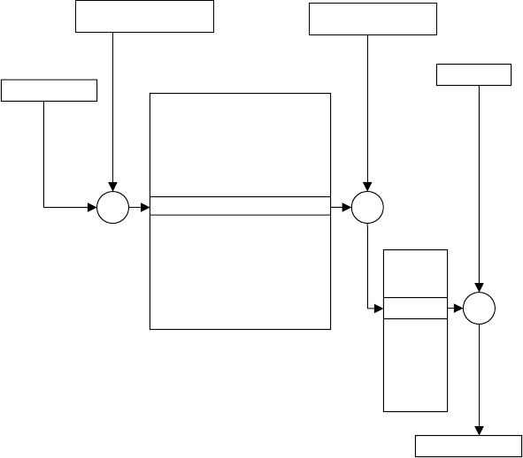
7.2.10. Pentium Memory Management
In the Pentium processor, both segmentation and paging are individually available
and can also be disabled. Four distinct views of the memory exist:
1. Unsegmented unpaged memory
2. Unsegmented paged memory
3. segmented unpaged memory
4. segmented paged memory
For segmentation, the 16-bit segment number (two of which are used for protection)
and the 32-bit offset produce a segmented virtual address space equal to 2
46
¼ 64
terabytes. The virtual address space is divided into two parts: one half, that is,
8K 4 GB, is global and shared by all processes, and the other half is local and
is distinct for each process.
For paging, a two-level table lookup paging system is used. First level is a page
directory with 1024 entries, that is, 1024 page groups, each with its own page table
and each FOUR MB in length. Each page table contains 1024 entries; each entry
corresponds to a single 4 KB page.
Segment Number
Segment Table
Offset
Displacement
Physical Segment Base Address
Page Table
Physical Address
Physical Address
Virtual Page Number
Σ
Σ
Σ
Figure 7.19 Paged segmentation address translation
7.2. VIRTUAL MEMORY 155

7.3. READ-ONLY MEMORY
Random access as well as cache memories are examples of volatile memories. A
volatile storage is defined as one that loses its contents when power is turned off.
Nonvolatile memory storages are those that retain the stored information if power
is turned off. As there is a need for volatile storage there is als o a need for nonvo-
latile storage. Computer system boot subroutines, microcode control, and video
game cartridges are a few examples of computer software that require the use of
nonvolatile storage. Read-only memory (ROM) can also be used to realize combi-
national logic functions.
The technology used for implementing ROM chips has evolved over the years. Early
implementations of ROMs were called mask-programmed ROMs. In this case, a made-
to-order one time ROM is programmed according to a specific encoding pattern sup-
plied by the user. The structure of a 44 CMOS ROM chip is shown in Figure 7.20.
In this figure an n-type transistor is placed where a 1 is to be stored. A two-to-four
address decoder is used to create four word lines; each is used to activate a row of
transistors. When a 1 appears on the word line, the corresponding transistors will be
turned on, thus pulling the corresponding bit line to 0. An inve rter at the output of the
Figure 7.20 Example of a 44 CMOS ROM chip
156
MEMORY SYSTEM DESIGN II

bit lines is used to output a 1 at the output of those pulled down bit lines. Table 7.3
shows the patterns stored at each of the four ROM locations.
Mask-programmed ROMs are primarily used to store machine microcode, desk-
top bootstrap loaders, and video game cartridges. Because they can be programmed
only once by the manufacturer, mask-programmed ROMs are inflexible. If the user
would like to program his/her ROM on site, then a different type of ROM, called the
Programmable ROM (PROM) should be used. In this case, fuses, instead of transis-
tors, are placed at the intersection of word and bit lines. Th e user can program the
PROM by selectively blowing up the appropriate fuses. This can be done by allow-
ing a high current to flow in those particular fuses, thus causing them to blow up.
This process is known as “burning the ROM.”
Although it allows for some added flexibility, PROM is still restricted by the fact
that it can only be programmed once (by the user). A third type of ROM, calle d
Erasable PROM (EPROM), is reprogrammable; that is, it allows stored data to be
erased and new data to be stored. In order to provide such flexibility, EPROMs
are constructed using a special type of transistors. These transistors are able to
assume one of two statuses, normal or disabled. A disabled transistor acts like a
switch that is turned off all the time. A normal transistor can be programmed to
become open all the time by inducing a certain amount of charge to be trapped
under its gate. A disabled transistor can become normal again by removing
the induced charge. This requires exposing those transistors to ultraviolet light.
Exposing the EPROM chip to such ultraviolet light will lead to the erasure of the
entire chip contents. This is considered a major drawback of EPROMs. Both
PROMs and EPROMs are used in prototyping, of moderate size systems.
Flash EPROMs (FEPROMs) have emerged as strong contenders to EPROMs.
This is because FEPROMs are more compact, faster, and removable compared to
EPROMs. The erasure time of a FEPROM is far faster than that of an EPROM.
A different type of ROM, which overcomes the drawback of the EPROM, is the
Electrically EPROM or EEPROM. In this case, the erasure of the EPROM can be
done electrically and, moreove r, selectively; that is, only the contents of selective
cells can be erased, leaving the other cells’ contents untouched. Both FEPROMs
and EEPROMs are used in applications requiring occasional updating of infor-
mation, such as Programmable TVs, VCR, and automotives.
Table 7.4 summarizes the main characteristics of the different types of ROM
discussed above.
TABLE 7.3 Patterns Stored at Four ROM Locations
Address
lines
Word line
activated
Output
pattern
00 W
0
1001
01 W
1
0110
10 W
2
1010
11 W
3
0101
7.3. READ-ONLY MEMORY 157

7.4. SUMMARY
The discussion in this chapter has been a continuation of that conducted in Chapter 6.
In particula r, this chapter has been dedicated to cover the design aspects that relat e to
the internal and external organization of the main memory. The design of a static
RAM cell was introduced with emphasis on the read and write operations. Our dis-
cussion on virtual memory started with the issues related to address translation.
Three address translation techniques were discussed and compared. These are the
direct, associative, and the set-associative techniques. The use of a TLB to improve
the average access time was explained. Three replacement techniques were intro-
duced. These are the FIFO, LRU, and clock replacement. Segmented paged systems
were also introdu ced. Our discussion on virtual memory ended with an explanation
of the virtual memory aspects of the Pentium IV processor. Toward the end of the
chapter, we have touched on a number of implementations for ROMs.
EXERCISES
1. Consider the case of a computer system employing both a cache and a paged
virtual memory as shown below (Fig. 7.21). One can analyze this system
through identifying FIVE combinations of accesses. What are these combi-
nations? Determine the probability and the access time in each case assuming
the following information. Compute also the overall average access ti me.
TLB address translation and search 25 ns
Cache search time to determine whether address in cache 25 ns
Cache access time 25 ns
Main memory access time 250 ns
Hard disk access time 100 ms
TLB hit ratio 0.9
Cache hit ratio 0.95
Main memory hit ratio 0.8
2. A 6464 array of words (elements) is to be “normalized” as follows. For each
row, the largest element is found and all elements of the row are divided by
TABLE 7.4 Characteristics of Different ROM Implementations
ROM type Cost Programmability
Typical
applications
Mask-programmed ROM Truly inexpensive Once at manufacture Microcode
PROM Inexpensive Once on site Prototyping
EPROM Moderate Many times Prototyping
FEPROM Expensive Many times VCR & TVs
EEPROM Truly expensive Many times VCR & TVs
158
MEMORY SYSTEM DESIGN II

this maximum value. Assume that each page in the virtual memory consists of
64 words, and that 2K words of the main memory are allocated for storing data
during this computation. Suppose that it takes 100 ms to load a page from the
disk into the main memory when a page fault occurs.
(a) Write a simple piece of code (in a nota tional form) that can perf orm the
above job.
(b) How many page faults would occur if the elements of the array are stored
in column order in the virtual memory?
(c) How many page faults would occur if the elements of the array are stored
in row order in the virtual memory?
(d) Estimate the total time needed to perform this normalization for both
arrangements (b) and (c).
3. Design a 64M8-bit memory using a number of 16M1-bit static RAM
chips. Assume that each individual chip has a chip select (
CS) line and a
read/write (R=
WW) line. Compute the number of chips required and show a
complete connection diagram of the designed memory.
4. Consider the following stream of page requests: 1,2,3,4,5,1,2,3,4,5,1,2,3,4,5.
Assume that the main memory consists of FOUR page frames. Show a trace
of the status of the page frames in the MM and estimate the hit ratio assuming
each of the following page replacement algorithms.
(a) FIFO
(b) LRU
(c) FINUFO
5. Consider the case of a two-dimensional 2020 array A. The array is stored
column-major. For FIVE main memory page frames, compute how many
Figure 7.21 Computer system with cache and paged virtual memory
EXERCISES 159
page faults are generated by the following array-initialization loop. Assume
that LRU replacement algorithm is used and that all frames are initially
empty. Assume also that the page size is 40 elements.
for I ¼ 1to20do
for J ¼ 1to20do
A[I, J] ¼ 0;
6. In this problem you are asked to pick a real-life computer memory system that
uses both caching and virtual memory schemes. Your job is to apply all the
knowledge that you have gained in this chapter concerning “Memory System
Design and Analysis” in describing and analyzing your selected system.
Examples that you may pick include but are not limited to Intel Pentium 4,
The PowerPC, Alpha AXP 21064, and so on. Use examples and illustrations
to support your analysis and be as specific as possible. Remember that the empha-
sis should be on the analysis and the basic design issues involved. You can use
any reference material but make sure that your include it in your reference list.
REFERENCES AND FURTHER READING
S. D. Burd, Systems Architecture, 3rd ed., Thomson Learning Ltd, Boston, 2001.
H. Cragon, Memory Systems and Pipelined Processors, Jones and Bartlett: Sudbury, MA,
1996.
V. C. Hamacher, Z. G. Vranesic, and S. G. Zaky, Computer Organization, 5th ed., McGraw-
Hill, NY, 2002.
J. L. Hennessy, and Patterson, D. A., Computer Architecture: A Quantitative Approach,
Morgan Kaufmann, San Francisco, CA, 1996.
V. P. Heuring, and H. F. Jordan, Computer Systems Design and Architecture, Addison-
Wesley, NJ, USA, 1997.
D. A. Patterson, and J. L. Hennessy, Computer Organization & Design: The Hardware/
Software Interface, Morgan Kaufmann, San Mateo, CA, 1994.
H. S. Stone, High-Performance Computer Architecture , Addison-Wesley, Amsterdam,
Netherlands, 1987.
B. Wilkinson, Computer Architecture: Design and Performance, Prentice-Hall,
Hertfordshire, UK, 1996.
Websites
http://www.sysopt.com
http://www.intel.com
http://www.AcerHardware.com
http://www.pmc-sierra.com/products/details/rm7000a
http://physinfo.ulb.ac.be/divers_html/PowerPC_Programming_Info/into_to_ppc/ppc2_
hardware.html
160
MEMORY SYSTEM DESIGN II

&
CHAPTER 8
Input–Output Design and Organization
Having considered the fundamental concepts related to instruction set design,
assembly language programming, processor design, and memory design, we now
turn our attenti on to the issues related to input–output (I/O) design and organiz-
ation. It should be emphasized at the outset that I/O plays a crucial role in any
modern computer system. Therefore, a clear understanding and appreciation of
the fundamentals of I/O operations, devices, and interfaces are of great importance.
Input–output (I/O) devices vary substantially in their characteristics. One dis-
tinguishing factor among input devices (and also among output devices) is their
data processing rate, defined as the average number of characters that can be pro-
cessed by a device per second. For example, while the data processing rate of an
input device such as the keyboard is about 10 characters (bytes)/second, a scanner
can send data at a rate of about 200,000 characters/second. Similarly, while a laser
printer can output data at a rate of about 100,000 characters/second, a graphic
display can output data at a rate of about 30,0 00,000 characters/second.
Striking a character on the keyboard of a computer will cause a character (in the
form of an ASCII code) to be sent to the computer. The amount of time passed
before the next character is sent to the computer will depend on the skill of the
user and even sometimes on his/her speed of thinking. It is often the case that the
user knows what he/she wants to input, but sometimes they need to think before
touching the next button on the keyboard. Therefore, input from a keyboard
is slow and burst in nature and it will be a waste of time for the computer to
spend its valuable time waiting for input from slow input devices. A mechanism
is theref ore needed whereby a device will have to interrupt the processor asking
for attention whenever it is ready. This is called interrupt-driven communication
between the computer and I/O devices (see Section 8.3).
Consider the case of a disk. A typical disk should be capable of transferring data
at rates exceeding several million bytes/second. It would be a waste of time to trans-
fer data byte by byte or even word by word. Therefore, it is always the case that data
is transferred in the form of blocks, that is, entire programs. It is also necessary
to provide a mechanism that allows a disk to transfer this huge volume of data
without the intervention of the CPU. This will allow the CPU to perform other
161
Fundamentals of Computer Organization and Architecture, by M. Abd-El-Barr and H. El-Rewini
ISBN 0-471-46741-3 Copyright # 2005 John Wiley & Sons, Inc.

useful operation(s) while a huge amount of data is being transferred between the disk
and the memory. This is the essence of the direct memory access (DMA) mechanism
discussed in Section 8.4.
We begin our discussion by offering some basic concepts in Section 8.1.
8.1. BASIC CONCEPTS
Figure 8.1 shows a simple arrangement for connecting the processor and the memory
in a given computer system to an input device, for example, a keyboard and an output
device such as a graphic display. A single bus consisting of the required address, data,
and control lines is used to connect the system’s components in Figure 8.1.
The way in which the processor and the memory exchange data has been
explained in Chapters 6 and 7. We are here concerned with the way the processor
and the I/O devices exchange data. It has been indicated in the introdu ction part
that there exists a big difference in the rate at which a processor can process infor-
mation and those of input and output devices. One simple way to accommodate this
speed difference is to have the input device, for example, a keyboard, deposit the
character struck by the user in a register (input register), which indicates the avail-
ability of that character to the processor. When the input character has been taken by
the processor, this will be indicated to the input device in order to proceed and input
the next character, and so on. Similarly, when the processor has a character to output
(display), it deposits it in a specific register dedicated for communication with the
graphic display (output register). When the character has been taken by the graphic
display, this will be indicated to the processor such that it can proceed and outpu t the
next character, and so on. This simple way of communication between the processor
and I/O devices, called I/O protocol, requires the availability of the input and
output registers. In a typical computer system, there is a number of input registers ,
each belonging to a specific input device. There is also a number of output registers ,
System Bus
Processor Memory
Output Device
(Graphic Display)
Input Device
(Keyboard)
Figure 8.1 A single bus system
162
INPUT– OUTPUT DESIGN AND ORGANIZATION

each belonging to a specific output device. In addition, a mechanism according to
which the processor can address those input and output registers must be adopted.
More than one arrangement exists to satisfy the abovementioned requirements.
Among these, two particular methods are explained below.
In the first arrangement, I/O devices are assigned particular addresses, isolated
from the address space assigned to the memory. The execu tion of an input instruc-
tion at an input device address will cause the character stored in the input register of
that device to be transferred to a specific register in the CPU. Similarly, the
execution of an output instruction at an output device address will cause the char-
acter stored in a specific register in the CPU to be transferred to the output register
of that output device. This arrangement, called shared I/O, is shown schematically
in Figure 8.2. In this case, the address and data lines from the CPU can be shared
between the memory and the I/O devices. A separate control line will have to be
used. This is because of the need for executing input and output instructions. In a
typical computer system, there exists more than one input and more than one
output device. Therefore, there is a need to have address decoder circuitry for
device identification. There is also a need for status registers for each input and
output device. The status of an input device, whether it is ready to send data to
the processor, should be stored in the status register of that device. Similarly, the
status of an output device, whether it is ready to receive data from the processor,
should be stored in the status register of that devi ce. Input (output) registers,
status registers, and address decoder circuitry represent the main components of
an I/O interface (module).
Address Bus
Data Bus
Memory Control Lines
Input Device(s) Control Lines
Output Device(s) Control Lines
Processor
Memory
Output Device
(Graphic Display)
Input Device
(Keyboard)
Figure 8.2 Shared I /O arrangement
8.1. BASIC CONCEPTS 163

The main advantage of the shared I/O arrangement is the separation between the
memory address space and that of the I/O devices. Its main disadvantage is the need
to h ave special input and output instructions in the processor instruction set. The
shared I/O arrangement is mostly adopted by Intel.
The second possible I/O arrangement is to deal with input and output registers as
if they are regular memory locations. In this case, a read operation from the address
corresponding to the input register of an input device, for example, Read Device 6,is
equivalent to performing an input operation from the input register in Device #6.
Similarly, a write operation to the address corresponding to the output register of
an output device, for example, Write Device 9, is equivalent to performing an
output operation into the output register in Device #9. This arrangement is called
memory-mapped I/O. It is shown in Figure 8.3.
The main advantage of the memory-mapped I/O is the use of the read and write
instructions of the processor to perform the input and output operations, respectively.
It eliminates the need for introducing special I/O instructions. The main disadvantage
of the memory-mapped I/O is the need to reserve a certain part of the memory address
space for addressing I/O devices, that is, a reduction in the available memory address
space. The memory-mapped I/O has been mostly adopted by Motorola.
8.2. PROGRAMMED I/O
In this section, we present the main hardware components required for communi-
cations between the processor and I/O devices. The way according to which such
Address Bus
Data Bus
Control Lines
Processor
Memory
Output Device
(Graphic Display)
Input Device
(Keyboard)
Figure 8.3 Memory-mapped I/O arrangement
164
INPUT– OUTPUT DESIGN AND ORGANIZATION

communications take place (protocol) is also indicated. This protocol has to be pro-
grammed in the form of routines that run under the control of the CPU. Consider, for
example, an input operation from Device 6 (could be the keyboard) in the case of
shared I/O arrangement. Let us also assume that there are eight different I/O
devices connected to the processor in this case (see Fig. 8.4).
The following protocol steps (program) have to be followed:
1. The processor executes an input instruction from device 6, for example,
INPUT 6. The effect of executing this instruction is to send the device
number to the addre ss decoder circuitry in each input device in order to ident-
ify the specific input device to be involved. In this case, the output of the deco-
der in Device #6 will be enabled, while the outputs of all other decode rs will
be disabled.
2. The buffers (in the figure we assumed that there are eight such buffers) holding
the data in the specified input device (Device #6) will be enabled by the output
of the address decoder circuitry.
3. The data output of the enabled buffers will be available on the data bus.
Figure 8.4 Example eight-I/O device connection to a processor
8.2. PROGRAMMED I/O 165

4. The instruction decoding will gate the data available on the data bus into the
input of a particular register in the CPU , normally the accumulator.
Output operations can be performed in a way similar to the input operation
explained above. The only difference will be the direction of data transfer, which
will be from a specific CPU register to the output register in the specified output
device. I/O operations performed in this manner are called programmed I/O.
They are performed under the CPU control. A complete instruction fetch, decode,
and execute cycle will have to be executed for every input and every output oper-
ation. Programmed I/O is useful in cases whereby one character at a time is to be
transferred, for example, keyboard and character mode printers. Although simple,
programmed I/O is slow.
One point that was overlooked in the above description of the programmed I/Ois
how to handle the subst antial speed difference between I/O devices and the pro-
cessor. A mechanism should be adopted in order to ensure that a character sent to
the output register of an output device, such as a screen, is not overwritten by the
processor (due to the processor’s high speed ) before it is displayed and that a char-
acter available in the input register of a keyboard is read only once by the processor.
This brings up the issue of the status of the input and output devices. A mechanism
that can be implemented requires the availability of a Status Bit ( B
in
) in the interface
of each input device and Status Bit (B
in
) in the interface of each output device.
Whenever an input device such as a keyboard has a character available in its
input register, it indicates that by setting B
in
¼ 1. A program in the processor can
be used to continuously monitor B
in
. When the program sees that B
in
¼ 1, it will
interpret that to mean a character is available in the input register of that device.
Reading such character will require executing the protocol explained above. When-
ever the character is read, then the program can reset B
in
¼ 0, thus avoiding multiple
read o f the same character. In a similar manner, the processor can deposit a character
in the output register of an output device such as a screen only when B
out
¼ 0. It is
only after the screen has displayed the character that it sets B
out
¼ 1, indicating to
the program that monitors B
out
that the screen is ready to receive the next character.
The process of checking the status of I/O devices in order to determine their readi-
ness for receiving and/or sending characters, is called software I/O polling.Ahard-
ware I/O polling scheme is shown in Figure 8.5.
Figure 8.5 Hardware polling scheme
166
INPUT– OUTPUT DESIGN AND ORGANIZATION

In the figure, each of the N I/O devices has access to the interrupt line INR.
Upon recognizing the arrival of a request (called Interrupt Request) on
INR, the pro-
cessor polls the devices to determine the requesting device. This is done through
thedLog
2
Nepolling lines. The priority of the requesting device will determine the
order in which addresses are put on the polling lines. The address of the highest priority
device is put first, followed by the next priority, and so on until the least priority device.
In addition to the I/O polling, two other mechanisms can be used to carry out I/O
operations. These are interrupt-driven I/O and direct memory access (DMA). These
are discussed in the next two sections.
8.3. INTERRUPT-DRIVEN I/O
It is often necessary to have the normal flow of a program interrupted, for example, to
react to abnormal events, such as power failure. An interrupt can also be used to
acknowledge the completion of a particular course of action, such as a printer indicating
to the computer that it has completed printing the character(s) in its input register and
that it is ready to receive other character(s). An interrupt can also be used in time-sharing
systems to allocate CPU time among different programs. The instruction sets of modern
CPUs often include instruction(s) that mimic the actions of the hardware interrupts.
When the CPU is interrupted, it is required to discontinue its current activity,
attend to the interrupting condition (serve the interrupt), and then resume its activity
from wherever it stopped. Discon tinuity of the processor’s current activity requires
finishing executing the current instruction, saving the processor status (mostly in the
form of pushing register values onto a stack), and transferring control (jump) to what
is called the interrupt service routine (ISR). The service offered to an interrupt will
depend on the source of the interrupt. For example, if the interrupt is due to power
failure, then the action taken will be to save the values of all processor registers and
pointers such that resumption of correct operation can be guaranteed upon power
return. In the case of an I/O interrupt, serving an interrupt means to perform the
required data transfer. Upon finishing serving an interrupt, the processor should
restore the original status by popping the relevant values from the stack. Once the
processor returns to the normal state, it can enable sources of interrupt again.
One important point that was overlooked in the above scenario is the issue of ser-
ving multiple interrupts, for example, the occurrence of yet another interrupt while
the processor is currently serving an interrupt. Response to the new interrupt will
depend upon the priority of the newly arrived interrupt with respect to that of the
interrupt being currently served. If the newly arrived interrupt has priority less
than or equal to that of the currently served one, then it can wait until the processor
finishes serving the current interrupt. If, on the other hand, the newly arrived inter-
rupt has priority higher than that of the currently served interrupt, for example,
power failure interrupt occurring while serving an I/O interrupt, then the processor
will have to push its status onto the stack and serve the higher priority interrupt.
Correct handling of multiple interrupts in terms of storing and restoring the correct
processor status is guaranteed due to the way the push and pop operations are
8.3. INTERRUPT-DRIVEN I/O 167

performed. For example, to serve the first interrupt, STATUS 1 will be pushed onto
the stack. Upon receiving the second interrupt , STATUS 2 will be pushed onto the
stack. Upon serving the second interrupt, STATUS 2 will be popped out of the stack
and upon serving the first interrupt, STATUS 1 will be popped out of the stack.
It is possible to have the interrupting device iden tify itself to the processor by
sending a code following the interrupt request. The code sent by a given I/O
device can represent its I/O address or the memory address location of the start
of the ISR for that device. This scheme is called vectored interrupt.
8.3.1. Interrupt Hardware
In the above discussion, we have assumed that the processor has recognized the
occurrence of an interrupt before proceeding to serve it. Computers are provided
with interrupt hardware capability in the form of specialized interrupt lines to the
processor. These lines are used to send interrupt signals to the processor. In the
case of I/O, there exists more than one I/O device. The processor should be pro-
vided with a mechanism that enables it to handle simultaneous interrupt requests
and to recognize the interrupting device. Two basic schemes can be implemented
to achieve this task. The first scheme is called daisy chain bus arbitration
(DCBA) and the second is called independent source bus arbitration (ISBA).
According to the DCBA (see Fig. 8.6a), I/O devices present their interrupt
requests to the interrupt request line
INR (similar to the polling arrangement).
Upon recognizing the arrival of an interrupt request, the processor, through a
daisy chained grant line (GL), sends its grant to the requesting device to start com-
munication with the processor. The GL goes through all devices starting from the
first device nearer to the processor and going to the next device and so on until it
reaches the last device (Device #N). If Device #1 has put a request, then it will
hold the grant signal and start communication with the processor. If, on the other
hand, Device #1 has no interrupt request, it will pass the grant signal to device
#2, which will repeat the same procedure, and so on. In the case of multiple requests,
the DCBA arrangement gives highest priority to the device physically nearer to the
processor. The furthest device from the processor has the lowest priority.
According to the ISBA (see Fig. 8.6b), each I/O device has its own interrupt request
line, through which it can send its interrupt request, independent of the other devices.
Similarly, each I/O device has its own grant line, through which it receives the grant
signal for its request such that it can start communicating with the processor. I/O
device priority in the ISBA does not depend on the device location. A priority arbitra-
tion circuitry is needed in order to deal with simultaneous interrupt requests.
8.3.2. Interrupt in Operating Systems
When an interrupt occurs, the operating system gains control. The operating
system saves the state of the interrupted process, analyzes the interrupt, and
passes control to the appropriate routine to handle the interrupt. There are several
168 INPUT– OUTPUT DESIGN AND ORGANIZATION

types of interrupts, including I/O interrupts. An I/O interrupt notifies the operating
system that an I/O device has completed or suspended its operation and needs some
service from the CPU. To process an interrupt, the context of the current process
must be saved and the interrupt handling routine must be invoked. This process is
called context switching. A process context has two parts: processor context and
memory context. The processor context is the state of the CPU’s registers including
program counter (PC), program status words (PSWs), and other registers. The
memory context is the state of the program’s memory including the program
and data. The interrupt handler is a routine that processes each different type of
interrupt.
The operating system must provide programs with save area for their contexts. It
also must provide an organized way for allocating and deallocating memory for the
interrupted process. When the interrupt handling routine finishes processing the inter-
rupt, the CPU is dispatched to either the interrupted process, or to the highest priority
ready process. This will depend on whether the interrupted process is preemptive or
nonpreemptive. If the process is nonpreemptive, it gets the CPU again. First the con-
text must be restored, then control is returned to the interrupts process.
Figure 8.6 Interrupt hardware schemes. (a ) Daisy chain interrupt arrangement
(b) Independent interrupt arrangement
8.3. INTERRUPT-DRIVEN I/O 169

Figure 8.7 shows the layers of software involved in I/O operations. First, the pro-
gram issues an I/O request via an I/O call. The request is passed through to the I/O
device. When the device completes the I/O, an interrupt is sent and the interrupt handler
is invoked. Eventually, control is relinquished back to the process that initiated the I/O.
Example 1: 80386 Interrupt Architecture The 8086 processors have just
two hardware interrupt pins. These are labeled INTR and NMI. NMI is a nonmaskable
interrupt, which means it cannot be blocked and the processor must respond to it. The
NMI input is usually reserved for critical system functions. The INTR input is a mask-
able interrupt request line between the CPU and the programmable interrupt controller
(8259A PIC). Interrupts on INTR can be enabled and disabled using the instructions
STI (set interrupt flag) and CLI (clear interrupt flag), respectively.
Interrupt handlers are called interrupt service routines (ISR). The address of each
interrupt service routine is stored in four consecutive memory locations in the inter-
rupt vector table (IVT). The IVT stores pointers to ISR for each type of interrupt.
When an interrupt occurs, an 8-bit type number is supplied to the processor,
which identifies the appropriate entry in this table.
When an interrupt is generated by a device, it goes to the PIC. Multiple interrupts
may be generated simultaneously. However, they are all buffered by the PIC. The
PIC decides which one of these interrupts should be forwarded to the CPU. To
inform the CPU that an outstanding interrupt is waiting to be processed, the PIC
sends an interrupt request (INTR) to the CPU, which then, at the appropriate
time, responds with an interrupt acknowledgment (INTA). At this time, PIC will
put an 8-bit interrupt type number associated with the device on the bus so that
the CPU can identify which interrupt handler to invoke. In the case when several
interrupts are pending, PIC wi ll send next interrupt request to the CPU only after
it receives an end of interr upt command from the current ISR. Figure 8.8 shows
the simple protocol that is used to determine which ISR is to be invoked.
In the computer designs that used a single PIC (PC and XT), eight different inter-
rupt reque sts are allowed (IRQ0–IRQ7). Table 8.1 shows a list of standard interrupt
type numbers for typical devices. When AT was designed, a second PIC was added,
Hardware
Device Independent Software
User Processes
I/O Request
I/O Reply
Perform I/O
Wakeup driver when I/O is done
Device Drivers
Interrupt Handlers
Figure 8.7 Layered I/O software
170
INPUT– OUTPUT DESIGN AND ORGANIZATION

increasing the number of interrupt inputs to 15. Figure 8.9 shows two PICS wired in
cascade. One PIC is designated as master and the other becomes the slave. As shown
in the figure, all slave interr upts are input via IRQ1 of the master. In general, eight
different slaves can be accommodated by a single PIC.
Example 2: ARM Interrupt Architecture ARM stands for Advanced RISC
Machines. ARM is a 16/32-bit architecture that is used for portable devices because
of its low power consumption and reasonable performance. Interrupt requests to the
ARM core are collected and controlled by the interrupt controller, which is called
ATIC. The interrupt controller provides an interface to the core and can collect
up to 64 interrupt requests.
The usual sequence of events for interrupts is as follows. Interrupts would be
enabled at the source (such as a peripheral), then enabled in the interrupt controller,
and finally, enabled to the core. When an interrupt occurs at the source, its signal is
routed to the interrupt controller then to the ARM core. In the interrupt controller,
the interrupt can be enabled or disabled to the core and can be assigned a priority
Device
8259A
PIC
CPU
ISR
1. IRQ# Interrupt
2. INTR
3. INTA
4. INT #
5. Invoke
8. Return
7. End Interrupt
6. Service
Figure 8.8 Interrupt handling in 8086
TABLE 8.1 Standard IBM-PC Interrupt Type Numbers
for Typical Devices
Device
IRQ
no.
Interrupt
type number
Programmable interval timer 0 08H
Keyboard 1 09H
Cascading to the second PICs 2 Reserved
Serial communication port (COM2) 3 0BH
Serial communication port (COM1) 4 0CH
Fixed disk controller 5 0DH
Floppy disk controller 6 0EH
Parallel printer controller 7 0FH
8.3. INTERRUPT-DRIVEN I/O 171

level. Once the interrupt request reaches the core, it will halt the core from its normal
processing routines to allow the interrupt request to be serviced.
Among the different interrupt requests that the ARM core can handle are IRQ and
FIQ requests. The IRQ (normal interrupt request) is used for gener al-purpose inter-
rupt handling. It has a lower priority than an FIQ (fast interrupt request) and is
masked out when an FIQ sequence is entered. The FIQ is used to support high-
speed data transfer or channel processes.
IRQ0
IRQ1
IRQ2
IRQ3
IRQ4
IRQ5
IRQ6
IRQ7
D0-D7
INT
Address bus
INTR
8259A Master
INTA
INTA
CS
SP/ EN
8259A Slave
IRQ8
IRQ9
IRQ10
IRQ11
IRQ12
IRQ13
IRQ14
IRQ15
D0-D7
INT
Address bus
INTA
CS
SP/ EN
Figure 8.9 Fifteen different interrupts are supported by two PICs wired in cascade
172
INPUT– OUTPUT DESIGN AND ORGANIZATION

Similar to the 8086, the addresses of the interrupt handlers are stored in a vector
table, which is shown in Table 8.2. For example, when an IRQ is detected by the core,
it accesses address 018 of the vector table and executes the instruction loaded in that
address. Normally, the instruction found at 018 of the vector table is of the form:
LDR PC, IRQ_Handler (load the address of the IRQ interrupt handler in the PC).
When an FIQ is detected by the core, it accesses address 01C of the vector table
and executes the instruction loaded in that address. Normally, the instruction found
at 01C of the vector table is of the form: LDR PC, FIQ_Handler.
When an interrupt occurs, the following happens inside the core:
1. The CPSR (current program state register) is copied to the SPSR (saved pro-
gram status register) of the mode being entered.
2. The CPSR bits are set as appropriate to the mode being entered, the core is set
to ARM state, and the relevant interrupt disable flags are set.
3. The appropriate set of banked registers are banked in.
4. The return address is stored in the link register (of the relevant mode).
5. The PC is set to the relevant vector address.
For example, when an IRQ interrupt is detected, the ARM core enables SPSR_irq as
the CPSR, enters the IRQ mode by setting the mode bits in the CSPR to 10010, dis-
ables Normal interrupts by setting the I bit in the CPSR, saves the address of the next
instruction R14_irq, and loads 018 into the PC. At address 018, an instruction
will load the address of the interrupt handler into the PC. Similarly, when an FIQ
interrupt is detected, the ARM core enables SPSR_fiq as the CPSR, enters the
FIQ mode by setting the mode bits in the CSPR to 10001, disables Normal and
Fast interrupts by setting the F and I b its in the CPSR, saves the address of the
next instruction R14_fiq, and loads 01C into the PC. At address 01C, an instruc-
tion will load the address of the interrupt handler into the PC.
MC9328MX1/MXL AITC The MC9328MX1/ MXL AITC contains twenty-six
32-bit registers, which are described in Table 8.3. Using these registers, the AITC
allows the selection of whether a pending interrupt source will create a Normal
interrupt (IRQ) or a Fast interrupt (FIQ) to the core. This is accomplished via the
TABLE 8.2 Interrupt Vector Table
Exception type Mode Address
Reset Supervisor 000000000
Undefined instructions Undefined 000000004
Software interrupts (SWI) Supervisor 000000008
Prefetch abort Abort 00000000C
Data abort Abort 000000010
IRQ (Normal interrupt) IRQ 000000018
FIQ (Fast interrupt) FIQ 00000001C
8.3. INTERRUPT-DRIVEN I/O 173

TABLE 8.3 The AITC Registers
Register Description
INTCNTL Configures specific control functions of the AITC.
NIMASK Controls the Normal interrupt mask level. All Normal interrupt
priority levels at or below what is programmed in the NIMASK
register will be masked. Normal interrupt priorities are
programmed via the NIPRIORITY[7 : 0] registers.
INTENNUM Provides hardware accelerated enabling of interrupts. This is done by
programming this register with the interrupt source that is desired
to be enabled. Doing so will immediately enable (set) this interrupt
source bit in the INTENABLEH/L register.
INTDISNUM Provides hardware accelerated disabling of interrupts. This is done
by programming this register with the interrupt source that is
desired to be disabled. Doing so will immediately disable (clear)
this interrupt source bit in the INTENABLEH/L register.
INTENABLEH Used to enable pending interrupt source bits [63–32] to the core.
INTENABLEL Used to enable pending interrupt source bits [31 –0] to the core.
INTTYPEH Used to select whether an enabled and pending interrupt source bit
[63–32] will create a Normal interrupt or Fast interrupt to the core.
INTTYPEL Used to select whether an enabled and pending interrupt source bit
[31–0] will create a Normal interrupt or Fast interrupt to the core.
NIPRIORITY[7 : 0] Provides software prioritization of Normal interrupts.
NIVECSR Provides the priority of the highest pending Normal interrupt and
provides the source number of the highest pending Normal interrupt.
FIVECSR Provides the source number of the highest pending Fast interrupt.
INTSRCH Reflects the status of interrupt request inputs (sources 63–32) into
the interrupt controller.
INTSCRL Reflects the status of interrupt request inputs (sources 31–0) into the
interrupt controller.
INTFRCH Allows for software generation of interrupts for interrupt sources 63
through 32.
INTFRCL Allows for software generation of interrupts for interrupt sources 31
through 0.
NIPNDH Reflects the source number(s) of pending Normal interrupt requests,
for interrupt sources 63 through 32.
NIPNDL Reflects the source number(s) of pending Normal interrupt requests,
for interrupt sources 31 through 0.
FIPNDH Reflects the source number(s) of pending Fast interrupt requests, for
interrupt sources 63 through 32.
FIPNDL Reflects the source number(s) of pending Fast interrupt requests, for
interrupt sources 31 through 0.
174
INPUT– OUTPUT DESIGN AND ORGANIZATION
INTTYPEH and INTTYPEL registers. Each bit in these registers corresponds to an
interrupt source available in the system. Setting a bit will select its corresponding
interrupt source as a Fast interrupt, whereas clearing this bit will select its corre-
sponding bit as a Normal interrupt. In the INTTYPEL register, bit 0 corresponds
to interrupt source 0, bit 1 corresponds to interrupt source 1, and so on up to bit
31, which corresponds to interrupt source 31. In the INTTYPEH register, bit 0 cor-
responds to interrupt source 32, bit 1 corresponds to interrupt source 33, and so on up
to bit 31, which corresponds to interrupt source 63.
After determining the type of the pending interrupt, the next step is to enable the
interrupt. This can be done via the INTENABLEH and INT ENABLEL registers. To
enable a pending interrupt to the core, its corresponding interrupt source b it in the
INTENABLEH or INTENABLEL must be set. Likewise, to disable the interrupt,
clear this bit. In the INTENABLEL register, bit 0 corresponds to interrupt source
0, bit 1 corresponds to interrupt source 1, and so on up to bit 31, which corresponds
to interrupt source 31. In the INTENABLEH register, bit 0 corresponds to interrupt
source 32, bit 1 corresponds to interrupt source 33, and so on up to bit 31, which
corresponds to interrupt source 63. For example, to select interrupt source bit 15
as a Normal interrupt, clear bit 15 in the INTTYPEL register. Then, to enable this
interrupt, set bit 15 in the INTENABLEL register. Likewise, to select interrupt
source bit 45 as a Fast interrupt, set bit 13 in the INTTYPEH register. Then, to
enable this interrupt, set bit 13 in the INTENABLEH. The AITC also allows the pro-
grammer to prioritize the pending Normal interrupt sources to one of 16 different
priority levels. This can be done in the NIPRIORITY[7:0] registers.
8.4. DIRECT MEMORY ACCESS (DMA)
The main idea of direct memory access (DMA) is to enable peripheral devices to cut
out the “middle man” role of the CPU in data transfer. It allows peripheral devices to
transfer data directly from and to memory without the intervention of the CPU. Having
peripheral devices access memory directly would allow the CPU to do other work,
which would lead to improved performance, especially in the cases of large transfers.
The DMA controller is a piece of hardware that controls one or more peripheral
devices. It allows devices to transfer data to or from the system’s memory without
the help of the processor. In a typical DMA transfer, some event notifies the DMA
controller that data needs to be transferred to or from memory. Both the DMA and
CPU use memory bus and only one or the other can use the memory at the same
time. The DMA controller then sends a request to the CPU asking its permission
to use the bus. The CPU returns an acknowledgment to the DMA controller granting
it bus access. The DMA can now take control of the bus to independently conduct
memory transfer. When the transfer is complete the DMA relinquishes its control of
the bus to the CPU. Processors that support DMA provide one or more input sign als
that the bus requester can assert to gain control of the bus and one or more output
signals that the CPU assert s to indicate it has relinquished the bus. Figure 8.10
shows how the DMA controller shares the CPU’s memory bus.
8.4. DIRECT MEMORY ACCESS (DMA) 175

Direct memory access controllers require initialization by the CPU. Typical setup
parameters include the address of the source area, the address of the destination area,
the length of the block, and whether the DMA controller should generate a processor
interrupt once the block transfer is complete. A DM A controller has an address reg-
ister, a word count register, and a control register. The address register contains an
address that specifies the memory location of the data to be transferred. It is typically
possible to have the DMA controller automatically increment the address register
after each word transfer, so that the next transfer will be from the next memory
location. The word count register holds the number of words to be transferred.
The word count is decremented by one after each word transfer. The control register
specifies the transfer mode.
Direct memory access data transfer can be performed in burst mode or single-
cycle mode. In burst mode, the DMA controller keeps control of the bus until all
the data has been transferred to (from) memory from (to) the peripheral device.
This mode of transfer is needed for fast devices where data transfer cannot be
stopped until the entire transfer is done. In single-cycle mode (cycle stealing), the
DMA controller relinquishes the bus after each transfer of one data word. This mini-
mizes the amount of time that the DMA controller keeps the CPU from controlling
the bus, but it requires that the bus request/acknowledge sequence be performed for
every single transfer. This overhead can result in a degradation of the performance.
The single-cycle mode is preferred if the system cannot tolerate more than a few
cycles of added interrupt latency or if the peripheral devices can buffer very large
amounts of data, causing the DMA controller to tie up the bus for an excessive
amount of time.
The following steps summarize the DMA operations:
1. DMA controller initiates data transfer.
2. Data is moved (increasing the address in memor y, and reducing the count of
words to be moved).
CPU
Memory
DMA
Controller
Device
DMA Acknowledgement
DMA Request
Control Signals
Data Bus
Address Bus
Figure 8.10 DMA controller shares the CPU’s memory bus
176
INPUT– OUTPUT DESIGN AND ORGANIZATION
3. When word count reaches zero, the DMA informs the CPU of the terminati on
by means of an interrupt.
4. The CPU regains access to the memory bus.
A DMA controller may have multiple channels. Each channel has associated with it
an address register and a count register. To initiate a data transfer the device driver
sets up the DMA channel’s address and count registers together with the direction of
the data transfer, read or write. While the transfer is taking place, the CPU is free to
do other things. When the transfer is complete, the CPU is interrupted.
Direct memory access channels cannot be shared between device drivers. A
device driver must be able to determine which DMA channel to use. Some devices
have a fixed DMA channel, while others are more flexible, where the device driver
can simply pick a free DMA channel to use.
Linux tracks the usage of the DMA channels using a vector of dma_chan data
structures (one per DMA channel). The dma_chan data structure contain s just two
fields, a pointer to a string describ ing the owner of the DMA channel and a flag indi-
cating if the DMA channel is allocated or not.
8.5. BUSES
A bus in computer terminology represents a physical connection used to carry a
signal from one point to another. The signal carried by a bus may represent address,
data, control signal, or power. Typically, a bus consists of a number of connections
running together. Each connection is called a bus line. A bus line is normally ident-
ified by a number. Related groups of bus lines are usually identified by a name. For
example, the group of bus lines 1 to 16 in a given computer system may be used to
carry the address of memory locations, and therefore are identified as address lines.
Depending on the signal carried, there exist at least four types of buses: address,
data, control, and pow er buses . Data buses carry data, control buses carry control
signals, and power buses carry the power-supply/ground voltage. The size
(number of lines) of the address, data, and control bus varies from one system to
another. Consider, for example, the bus connecting a CPU and memory in a give n
system, called the CPU bus. The size of the memor y in that system is 512M-
word and each word is 32 bits. In such system, the size of the address bus should
be log
2
(5122
20
) ¼ 29 lines, the size of the data bus should be 32 lines, and at
least one control line (
RR=W) should exist in that system.
In addition to carrying control signals, a cont rol bus can carry timing signals.
These are signals used to determine the exact timing for data transfer to and from
a bus; that is, they determine when a given computer system component, such as
the processor, memor y, or I / O devices, can place data on the bus and when they
can receive data from the bus. A bus can be synch ronous if data transfer over the
bus is controlled by a bus clock. The clock acts as the timing reference for all bus
signals. A bus is asynchronous if data transfer over the bus is based on the avail-
ability of the data and not on a clock signal. Data is transferred over an asynchronous
8.5. BUSES 177

bus using a technique called handshaking. The operations of synchronous and asyn-
chronous buses are explained below.
To understand the difference between synchronous and asynchronous, let us con-
sider the case when a master such as a CPU or DMA is the source of data to be trans-
ferred to a slave such as an I/O device. The following is a sequence of events
involving the master and slave:
1. Master: send request to use the bus
2. Master: request is granted and bus is allocated to master
3. Master: place address/data on bus
4. Slave: slave is selected
5. Master: signal data transfer
6. Slave: take data
7. Master: free the bus
8.5.1. Synchronous Buses
In synchronous buses, the steps of data transfer take place at fixed clock cycles.
Everything is synchronized to bus clock and clock signals are made available to
both master and slave. The bus clock is a square wave signal. A cycle starts at
one rising edge of the clock and ends at the next rising edge, which is the beginning
of the next cycle. A transfer may take multiple bus cycles depending on the speed
parameters of the bus and the two ends of the transfer.
One scenario would be that on the first clock cycle, the master puts an address on
the address bus, puts data on the data bus, and asserts the appropriate control lines.
Slave recognizes its address on the address bus on the first cycle and reads the new
value from the bus in the second cycle.
Synchronous buses are simple and easily implemented. However, when connect-
ing devices with varying speeds to a synchronous bus, the slowest device will deter-
mine the speed of the bus. Also, the synchronous bus length could be limit ed to
avoid clock-skewing problems.
8.5.2. Asynchronous Buses
There are no fixed clock cycles in asynchronous buses. Handshaking is used instead.
Figure 8.11 shows the handshaking protocol. The master asserts the data-ready line
1
2
3
4
1
2
3
4
Data-ready
Data-accept
Data Data DataData-Bus
Figure 8.11 Asynchronous bus timing using handshaking protocol
178
INPUT– OUTPUT DESIGN AND ORGANIZATION

(point 1 in the figure) until it sees a data-accept signal. When the slave sees a data-
ready signal, it will assert the data-accept line (point 2 in the figure). The rising of the
data-accept line will trigger the falling of the data-ready line and the removal of data
from the bus. The falling of the data-ready line (point 3 in the figure) will trigger the
falling of the data-accept line (point 4 in the figure). This handshaking, which is
called fully interlocked, is repeated until the data is completely transferred. Asyn-
chronous bus is appropriate for different speed devices.
8.5.3. Bus Arbitration
Bus arbitration is needed to resolve conflicts when two or more devices want to
become the bus master at the same time. In short, arbitration is the process of select-
ing the next bus master from among multiple candidates. Conflicts can be resolved
based on fairness or priority in a centralized or distributed mechanisms.
Centralized Arbitration In centralized arbitration schemes, a single arbiter is
used to select the next master. A simple form of centralized arbitration uses a bus
request line, a bus grant line, and a bus busy line. Each of these lines is shared by
potential masters, which are daisy-chained in a cascade. Figure 8.12 shows this
simple centralized arbitration scheme.
In the figure, each of the potential masters can submit a bus request at any time.
A fixed priority is set among the masters from left to right. When a bus request is
received at the central bus arbiter, it issues a bus grant by asserting the bus grant
line. When the potential master that is closest to the arbiter (potential master 1) sees
the bus grant signal, it checks to see if it had made a bus request. If yes, it takes over
the bus and stops propagation of the bus grant signal any further. If it has not made a
request, it will simple turn the bus grant signal to the next master to the right (potential
master 2), and so on. When the transaction is complete, the busy line is deasserted.
Instead of using shared request and grant lines, multiple bus request and bus grant
lines can be used. In one scheme, each master will have its own independent request
and grant line as shown in Figure 8.13. The central arbiter can employ any priority-
based or fairness-based tiebreaker. Another scheme allows the masters to have mul-
tiple priority levels. For each priority level, there is a bus reque st and a bus grant
line. Within each priority level, daisy chain is used. In this scheme, each device is
attached to the daisy chain of one priority level. If the arbiter receives multiple
Central
Bus
Arbiter
Potential
Master 1
Potential
Master 2
Potential
Master n
Bus Busy
Bus Request
Bus Grant
Figure 8.12 Centralized arbiter in a daisy-chain scheme
8.5. BUSES 179

bus requests from different levels, it grants the bus to the level with the highest
priority. Daisy chaining is used among the devices of that level. Figure 8.14
shows an example of four devices included in two priority levels. Potential
master 1 and potential master 3 are daisy-chained in level 1 and potential master
2 and potential master 4 are daisy-chained in level 2.
Decentralized Arbitration In decentralize d arbitration schemes, priority-based
arbitration is usually used in a distributed fashion. Each potential master has a
unique arbitration number, which is used in resolving conflicts when multiple
requests are submitted. For example, a conflict can always be resolve d in favor of
the device with the highest arbitration number. The question now is how to deter-
mine which device has the highest arbitration number? One method is that a request-
ing device would make its unique arbitration number available to all other devices.
Each device compares that number with its own arbitration number. The device with
the smaller number is always dismissed. Eventually, the requester with the highest
arbitration number will survive and be granted bus access.
Req-1
Grant-1
Req-2
Grant-2
Req-n
Grant-n
Central
Bus
Arbiter
Potential
Master 1
Potential
Master 2
Potential
Master n
Bus Busy
Figure 8.13 Centralized arbiter with independent request and grant lines
Central
Bus
Arbiter
Request level 1
Bus Busy
Request level 2
Grant level 1
Grant level 2
Potential
Master 1
Potential
Master 2
Potential
Master 3
Potential
Master 4
Figure 8.14 Centralized arbiter with two priority levels (four devices)
180
INPUT– OUTPUT DESIGN AND ORGANIZATION

8.6. INPUT–OUTPUT INTERFACES
An interface is a data path between two separate devices in a computer system. Inter-
face to buses can be classified based on the number of bits that are transmitted at a
given time to serial versus parallel ports. In a serial port, only 1 bit of data is trans-
ferred at a time. Mice and modems are usually connected to serial ports. A parallel
port allows more than 1 bit of data to be processed at once. Printers are the most
common peripheral devices connected to parallel ports. Table 8.4 shows a summary
of the variety of buses and interfaces used in personal computers.
TABLE 8.4 Descriptions of Buses and Interfaces Used in Personal Computers
Bus/Interface Description
PS/2 A type of port (or interface) that can be used to connect mice and
keyboards to the computer. The PS/2 port is sometimes called the
mouse port.
Industry standard
architecture (ISA)
ISA was originally an 8-bit bus and later expanded to a 16-bit bus in
1984. In 1993, Intel and Microsoft introduced a plug and play
ISA bus that allowed the computer to automatically detect and set
up computer ISA peripherals such as a modem or sound card.
Extended industry
standard
architecture
(EISA)
EISA is an enhanced form of ISA, which allows for 32-bit data
transfers, while maintaining support for 8- and 16-bit expansion
boards. However, its bus speed, like ISA, is only 8 MHz. EISA is
not widely used, due to its high cost and complicated nature.
Micro channel
architecture
(MCA)
MCA was introduced by IBM in 1987. It offered several additional
features over the ISA such as a 32-bit bus, automatically
configured cards and bus mastering for greater efficiency. It is
slightly superior to EISA, but not many expansion boards were
ever made to fit MCA specifications.
VESA (Video
electronics
standards
association) local
bus (VLB)
The VESA, a nonprofit organization founded by NEC, released the
VLB in 1992. It is a 32-bit bus that had direct access to the system
memory at the speed of the processor, commonly the 486 CPU
(33/40 MHz). VLB 2.0 was later released in 1994 and had a
64-bit bus and a bus speed of 50 MHz.
Peripheral
component
interconnect (PCI)
PCI was introduced by Intel in 1992, revised in 1993 to version 2.0,
and later revised in 1995 to PCI 2.1. It is a 32-bit bus that is also
available as a 64-bit bus today. Many modern expansion boards
are connected to PCI slots.
Advanced graphic
port (AGP)
AGP was introduced by Intel in 1997. AGP is a 32-bit bus designed for
the high demands of 3D graphics. AGP has a direct line to memory,
which allows 3D elements to be stored in the system memory
instead of the video memory. AGP is geared towards data-intensive
graphics cards, such as 3D accelerators; its design allows for data
throughput at rates of 266 MB/s.
(continued)
8.6. INPUT –OUTPUT INTERFACES 181

8.7. SUMMARY
One of the major features in a computer system is its ability to exchange data with
other devices and to allow the user to interact with the system. This chapter focused
on the I/O system and the way the processor and the I/O devices exchange data in a
computer system. The chapter described three ways of organizing I/O: programmed
I/O, interrupt-driven I/O, and DMA. In programmed I/O, the CPU handles the trans-
fers, which take place between registers and the devices. In interrupt-driven I/O, CPU
handles data transfers and an I/O module is running concurrently. In DMA, data are
transferred between memory and I/O devices without intervention of the CPU. We
also studied two methods for synchronization: polling and interrupts. In polling, the
processor polls the device while waiting for I/O to complete. Clearly processor
cycles are wasted in this method. Using interrupts, processors are free to switch to
other tasks during I/O. Devices assert interrupts when I/O is complete. Interrupts
TABLE 8.4 Continued
Bus/Interface Description
Universal serial bus
(USB)
USB is an external bus developed by Intel, Compaq, DEC, IBM,
Microsoft, NEC and Northern Telcom. It was released in 1996 with
the Intel 430HX Triton II Mother Board. USB has the capability of
transferring 12 Mbps, supporting up to 127 devices. Many devices
can be connected to USB ports, which support plug and play.
FireWire (IEEE
1394)
FireWire is a type of external bus, which supports very fast transfer
rates: 400 Mbps. Because of this, FireWire is suitable for
connecting video devices, such as VCRs, to the computer.
Small computer
system interface
(SCSI)
SCSI is a type of parallel interface that is commonly used for mass
storage devices. SCSI can transfer data at rates of 4 MB/s; in
addition, there are several varieties of SCSI that support higher
speeds: Fast SCSI (10 MB/s), Ultra SCSI and Fast Wide SCSI
(20 MB/s), as well as Ultra Wide SCSI (40 MB/s).
Integrated drive
electronics (IDE)
IDE is a commonly used interface for hard disk drives and
CD-ROM drives. It is less expensive than SCSI, but offers
slightly less in terms of performance.
Enhanced integrated
drive electronics
(EIDE)
EIDE is an improved version of IDE, which offers better
performance than standard SCSI. It offers transfer rates between
4 and 16.6 MB/s.
PCI-X PCI-X is a high performance bus that is designed to meet the
increased I/O demands of technologies such as Fibre Channel,
Gigabit Ethernet, and Ultra3 SCSI.
Communication and
network riser
(CNR)
CNR was introduced by Intel in 2000. It is a specification that
supports audio, modem USB and local area networking interfaces
of core logic chipsets.
182
INPUT– OUTPUT DESIGN AND ORGANIZATION
incurs some delay penalty. Two examples of interrupt handling were covered: 8086
family and ARM. The chapter also covered buses and interfaces. A wide variety of
interfaces and buses used in personal computers are summarized.
EXERCISES
1. Conduct an Internet search on I/O devices and prepare a table categorizing
the different devices into separate categories, for example input, output,
character-based, block-based, and so on. For every entry in the table, indicate
its speed, interface, and category.
2. What are the advantages and disadvantages of isolated versus memory
mapped I/O.
3. Show how data transfer from disk to memory is conducted under each of the
following I/O schemes: programmed I/O, interrup t-driven I/O, and DMA.
Show the steps taken in each case.
4. If an interrupt requires 50 ms of overhead time, and polling requires 5 ms per
device, describe different situations where each seems better than the other.
5. What entities in a computer system does a d evice driver communicate with?
What are the functions of a device driver? List all operations.
6. What types of operations is DMA used to accelerate?
7. A DMA module is transferring data to memory using cycle stealing from a
device that transmits data at rate of 19,200 bits per second. The speed of
the CPU is 3 MIPS. By how much would the DMA module affect the perform-
ance of the CPU.
8. Describe the scenarios in which a synchronous bus would outperform an asyn-
chronous bus and vice versa.
9. Discuss the advantages and disadvantages of the different bus arbitration
policies covered in the chapter. Prepare a contract table that compares the
arbitration techniques from both the implementation and operational
aspects.
REFERENCES AND FURTHER READING
I. Englander, The Architecture of Computer Hardware and System Software, John Wiley,
New York, 1996.
C. Hamacher, Z. Vranesic, and S. Zaky, Computer Organization, 5th ed., McGraw-Hill,
New York, 2002.
V. Heuring, and H. Jordan, Computer Systems Design and Architecture, Addison Wesley, NJ,
USA, 1997.
S. Shiva, Computer Design and Architecture , Harper Collins, MA, USA, 1991.
A. Tanenbaum, Structured Computer Organization, 4th ed., Prentice Hall, NJ, USA, 1999.
REFERENCES AND FURTHER READING 183
J. Uffenbeck, The 8086 Family, Design, Programming, and Interfacing, 3rd ed., Prentice
Hall, Essex, UK, 2002.
Websites
PCI Local Bus Specifications, www.pcisig.com/developers
SCSI-3 Architecture Model (SAM), www.ansi.org
Universal Serial Bus Specification, www.usb.org/developers
www.arm.com
www.motorola.com/semiconductors
184
INPUT– OUTPUT DESIGN AND ORGANIZATION

&
CHAPTER 9
Pipelining Design Techniques
There exist two basic techniques to increase the instruction execution rate of a pro-
cessor. These are to increase the clock rate, thus decreasing the instru ction execution
time, or alternatively to increase the number of instructions that can be executed
simultaneously. Pipelining and instruction-level parallelism are examples of the
latter technique. Pipelining owes its origin to car assembly lines. The idea is to
have more than one instruction being processed by the processor at the same
time. Similar to the assembly line, the success of a pipeline depends upon dividing
the execution of an instruction among a number of subunits (stages), each perform-
ing part of the required operations. A possible division is to consider instruction
fetch (F), instruction decode (D), operand fetch (F), instruction execu tion (E ),
and store of results (S) as the subtasks needed for the execution of an instru ction.
In this case, it is possible to have up to five instructions in the pipeline at the
same time, thus reducing instruction execu tion latency. In this Chapter, we discuss
the basic concepts involved in designi ng instruction pipelines. Performance
measures of a pipeline are introduced. The main issues contributing to instruction
pipeline hazards are discussed and some possible solutions are introduced. In
addition, we introduce the concept of arithmetic pipelining together with the prob-
lems involved in designing such a pipeline. Our coverage concludes with a review of
a recent pipeline processor.
9.1. GENERAL CONCEPTS
Pipelining refers to the technique in which a given task is divided into a number of
subtasks that need to be performed in sequence. Each subtask is performed by a
given functional unit. The units are connected in a serial fashion and all of them
operate simultaneously. The use of pipelining improves the performance compared
to the traditional sequential execution of tasks. Figure 9.1 shows an illustration of the
basic difference between executing four subtasks of a given instruction (in this case
fetching F, decoding D, execution E, and writing the results W) using pipelining and
sequential processing.
185
Fundamentals of Computer Organization and Architecture, by M. Abd-El-Barr and H. El-Rewini
ISBN 0-471-46741-3 Copyright # 2005 John Wiley & Sons, Inc.

It is clear from the figure that the total time required to process three instruc-
tions (I
1
, I
2
, I
3
) is only six time units if four-stage pipelining is used as compared
to 12 time units if sequential processing is used. A possible saving of up to 50%
in the execution time of these three instructions is obtained. In order to formulate
some performance measures for the goodness of a pipeline in processing a series of
tasks, a space time chart (called the Gantt’s chart) is used. The chart shows the suc-
cession of the subtasks in the pipe with respect to time. Figure 9.2 shows a Gantt’s
chart. In this chart, the vertical axis represents the subunits (four in this case) and
the horizontal axis represents time (measured in terms of the time unit required
for each unit to perform its task). In developing the Gantt’s chart, we assum e
that the time (T) taken by each subunit to perform its task is the same; we call
this the unit time.
As can be seen from the figure, 13 time units are needed to finish executing 10
instructions (I
1
to I
10
). This is to be compared to 40 time units if sequential proces-
sing is used (ten instructions each requiring four time units).
In the following analysis, we provide three performance measures for the good-
ness of a pipeline. These are the Speed-up S(n), Throughput U(n), and Efficiency
E(n). It should be noted that in this analysis we assume that the unit time T ¼ t
units.
1. Speed-up S(n) Consider the execution of m tasks (instructions) using
n-stages (units) pipeline. As can be seen, n þ m 1 time units are required
(a) Sequential Processing
I
1
I
1
I
2
I
3
I
2
I
3
Time
F1 D1 E1 W1
F1 D1 E1 W1
F2 D2 E2 W2
F2 D2 E2 W2
F3 D3 E3 W3
F3
123456789101112
D3 E3 W3
(b) Pipelining
Figure 9.1 Pipelining versus sequential processing
U
4
U
3
U
2
U
1
I
1
I
2
I
3
I
4
I
5
I
6
I
7
I
8
I
9
I
10
I
1
I
2
I
3
I
4
I
5
I
6
I
7
I
8
I
9
I
10
I
1
I
2
I
3
I
4
I
5
I
6
I
7
I
8
I
9
I
10
I
1
I
2
I
3
I
4
I
5
I
6
I
7
I
8
I
9
I
10
12345678910111213
Time
Figure 9.2 The space –time chart (Gantt chart)
186
PIPELINING DESIGN TECHNIQUES

to complete m tasks.
Speed-up S(n) ¼
Time using sequential processing
Time using pipeline processing
¼
m n t
(n þ m 1) t
¼
m n
n þ m 1
Lim
m!1
S(n) ¼ n (i:e:, n-fold increase in speed is theoretically possible)
2. Throughput U(n)
Throughput U(n) ¼ no: of tasks executed per unit time ¼
m
(n þ m 1) t
Lim
m!1
U(n ) ¼ 1 assuming that t ¼ 1 unit time
3. Efficiency E(n)
Efficiency E(n) ¼ Ratio of the actual speed-up to the maximum speed-up
¼
Speed-up
n
¼
m
n þ m 1
Lim
m!1
E(n) ¼ 1
9.2. INSTRUCTION PIPELINE
The simple analysis made in Section 9.1 ignores an important aspect that can affect
the performance of a pipeline, that is, pipeline stall. A pipeline operation is said to
have been stalled if one unit (stage) requires more time to perform its function, thus
forcing other stages to become idle. Consider, for example, the case of an instruction
fetch that incu rs a cache miss. Assume also that a cache miss requires three extra
time units. Figure 9.3 illustrates the effect of having instruction I
2
incurring a
cache miss (assuming the execution of ten instructions I
1
to I
10
).
U
4
U
3
U
2
U
1
I
1
I
1
I
1
I
2
I
3
I
4
I
5
I
6
I
7
I
8
I
9
I
10
I
2
I
3
I
4
I
5
I
6
I
7
I
8
I
9
I
10
I
2
I
3
I
4
I
5
I
6
I
7
I
8
I
9
I
10
I
3
I
1
I
2
I
4
I
5
I
6
I
7
I
8
I
9
I
10
123456789101112 1413 15 16
Figure 9.3 Effect of a cache miss on the pipeline
9.2. INSTRUCTION PIPELINE 187

The figure shows that due to the extra time units needed for instruction I
2
to be
fetched, the pipeline stalls, that is, fetching of instruction I
3
and subsequent instruc-
tions are delayed. Such situations create what is known as pipeline bubble (or pipe-
line hazards). The creation of a pipeline bubble leads to wasted unit times, thus
leading to an overall increase in the number of time units needed to finish executing
a given number of instructions. The number of time units needed to execute the 10
instructions shown in Figure 9.3 is now 16 time units, compare d to 13 time units if
there were no cache misses.
Pipeline hazards can take place for a number of other reasons. Among these are
instruction dependency and data dependency. These are explained below.
9.2.1. Pipeline “Stall” Due to Instruction Dependency
Correct operation of a pipeline requires that operation performed by a stage MUST
NOT depend on the opera tion(s) performed by other stage(s). Instruction depen-
dency refers to the case whereby fetching of an instruction depends on the results
of executing a previous instruction. Instruction dependency manifests itself in the
execution of a conditional branch instruction. Consider, for example, the case of a
“branch if negative” instruction. In this case, the next instruction to fetch will not
be known until the result of execu ting that “branch if negative” instruction is
known. In the following discussion, we will assume that the instruction following
a conditional branch instruction is not fetched until the result of executing the
branch instruction is known (stored). The following example shows the effect of
instruction dependency on a pipeline.
Example 1 Consider the execution of ten instructions I
1
–I
10
on a pipeline con-
sisting of four pipeline stages: IF (instruction fetch), ID (instruction decode), IE
(instruction execute), and IS (instruction resu lts store). Assume that the instruction
I
4
is a conditional branch instruction and that when it is executed, the branch is
not take n, that is, the branch condition(s) is(are) not satisfied. Assume also that
when the branch instruction is fetched, the pipeline stalls until the result of executing
the branch instruction is stored. Show the succession of instructions in the pipeline;
that is, show the Gantt’s chart. Figure 9.4 shows the required Gantt’s chart. The
bubble created due to the pipeline stall is clearly shown in the figure.
IS
IE
ID
IF
I
1
I
1
I
1
I
2
I
3
I
4
I
5
I
6
I
7
I
8
I
9
I
10
I
2
I
3
I
4
I
5
I
6
I
7
I
8
I
9
I
10
I
2
I
3
I
4
I
5
I
6
I
7
I
8
I
9
I
10
I
1
I
2
I
3
I
4
I
5
I
6
I
7
I
8
I
9
I
10
123456789101112 1413 15 16
Figure 9.4 Instruction dependency effect on a pipeline
188
PIPELINING DESIGN TECHNIQUES

9.2.2. Pipeline “Stall” Due to Data Dependency
Data dependency in a pipeline occurs when a source operand of instruction
I
i
depends on the results of executing a preceding instruction, I
j
, i . j. It should
be noted that although instruction I
i
can be fetched, its operand(s) may not be avail-
able until the results of instruction I
j
are stored. The following example shows the
effect of data dependency on a pipeline.
Example 2 Consider the execution of the following piece of code:
†
ADD R
1
, R
2
, R
3
; R
3
R
1
þ R
2
SL R
3
; R
3
SL(R
3
)
SUB R
5
, R
6
, R
4
; R
4
R
5
2 R
6
†
In this piece of code, the first instruction, call it I
i
, adds the contents of two registers
R
1
and R
2
and stores the result in register R
3
. The second instruction, call it I
iþ1
,
shifts the contents of R
3
one bit position to the left and stores the result back
into R
3
. The third instruction, call it I
iþ2
, stores the result of subtracting the content
of R
6
from the content of R
5
in register R
4
. In order to show the effect of such data
dependency, we will assume that the pipeline consists of five stages, IF, ID, OF, IE,
and IS. In this case, the OF stage represents the operand fetch stage. The functions of
the remaining four stages remain the same as explained before. Figure 9.5 shows the
Gantt’s chart for this piece of code. As shown in the figure, although instruction I
iþ1
has been successfully decoded during time unit k þ 2, this instruction cannot pro-
ceed to the OF unit during time unit k þ 3. This is because the operand to be fetched
by I
iþ1
during time unit kþ3 should be the content of register R
3
, which has been
modified by execution of instruction I
i
. However, the modified value of R
3
will
not be available until the end of time unit k þ 4. This will require instruction I
iþ1
to wait (at the output of the ID unit) until k þ 5. Notice that instruction I
iþ2
will
IS
IE
OF
ID
IF
I
i
I
i
I
i
I
i
I
i
I
i+1
I
i+1
I
i+2
kk + 1 k + 2 k + 3 k + 4 k + 5 k + 6
I
i+2
I
i+2
I
i+2
I
i+2
I
i+1
I
i+1
I
i+1
Time
Figure 9.5 The write-after-write data dependency
9.2. INSTRUCTION PIPELINE 189

have also to wait (at the output of the IF unit) until such time that instruction I
iþ1
proceeds to the ID. The net result is that pipeline stall takes place due to the data
dependency that exists between instruction I
i
and instruction I
iþ1
.
The data dependency presented in the above example resulted because register R
3
is the destination for both instructions I
i
and I
iþ1
. This is called a write-after-write
data dependency. Taking into consideration that any register can be written into
(or read from), then a total of four different possibi lities exist, including the
write-after-write case. The other three cases are read-after-write, write-after-read,
and read-after-read. Among the four cases, the read-after-read case should not
lead to pipeline stall. This is because a regist er read operation does not change
the content of the register. Among the remaining three cases, the write-after-write
(see the above example) and the read-after-write lead to pipeline stall. The following
piece of code illustrates the read-after-write case:
†
ADD R
1
, R
2
, R
3
; R
3
R
1
þ R
2
SUB R
3
,1,R
4
; R
4
R
3
2 1
†
In this case, the first instruction modifies the content of register R
3
(through a
write operation) while the second instruction uses the modified contents of R
3
(through a read operation) to load a value into regist er R
4
. While these two
instructions are proceeding within a pipeline, care should be taken so that the
value of register R
3
read in the second instruction is the updated value resulting
from execution of the previous instruction. Figure 9.6 shows the Gantt’s chart for
this case assuming that the first instruction is called I
i
and the second instruction
is called I
iþ1
.
It is clear that the operand of the second instruction cannot be fetched during time
unit kþ3 and that it has to be delayed until time unit k þ 5. This is because the modi-
fied value of the content of register R
3
will not be available until time slot k þ 5.
IS
IE
OF
ID
IF
I
i
I
i
I
i
I
i
I
i
I
i+1
I
i+1
kk + 1 k + 2 k + 3 k + 4 k + 5 k + 6
I
i+1
I
i+1
I
i+1
Time
Figure 9.6 The read-after-write data dependency
190
PIPELINING DESIGN TECHNIQUES

Fetching the operand of the second instruction during time slot k þ 3 will lead to
incorrect results.
Example 3 Consider the execution of the following sequence of instructions on a
five-stage pipeline consisting of IF, ID, OF, IE, and IS. It is required to show the
succession of these instructions in the pipeline.
I
1
! Load 21, R1; R1 21;
I
2
! Load 5, R2; R2 5;
I
3
! Sub R2, 1, R2 R2 R2 2 1;
I
4
! Add R1, R2, R3; R3 R1 þ R2;
I
5
! Add R4, R5, R6; R6 R4 þ R5;
I
6
! SL R3 R3 SL (R3)
I
7
! Add R6, R4, R7; R7 R4 þ R6;
In this example, the following data dependencies are observed:
Instructions Type of data dependency
I
3
and I
2
Read-after-write and write-after-write (W-W)
I
4
and I
1
Read-after-write (R-W)
I
4
and I
3
Read-after-write (R-W)
I
6
and I
4
Read-after-write and write-after-write (W-W)
I
7
and I
5
Read-after-write (R-W)
Figure 9.7 illustrates the progression of these instructions in the pipeline taking
into consideration the data dependencies mentioned above. The assumption made
in constructing the Gantt’s chart in Figure 9.7 is that fetching an operand by an
instruction that depends on the results of a previous instruction execution is delayed
until such operand is available, that is, the result is stored. A total of 16 time units are
required to execute the given seven instructions taking into consideration the data
dependencies among the different instructions.
IS
IE
OF
ID
IF
I
1
I
1
I
1
I
2
I
1
I
2
I
3
I
3
I
3
I
4
I
5
I
5
I
6
I
2
I
4
I
5
I
4
I
6
I
7
I
6
I
7
I
7
I
2
I
3
I
4
I
5
I
6
I
7
I
1
I
2
I
3
I
4
I
5
I
6
I
7
123456789101112 1413 15 16
Figure 9.7 Gantt’s chart for Example 3
9.2. INSTRUCTION PIPELINE 191

Based on the results obtained above, we can compute the speed-up and the
throughput for executing the piece of code given in Example 3 as:
Speed-up S(5) ¼
Time using sequential processing
Time using pipeline processing
¼
7 5
16
¼ 2:19
Throughput U(5) ¼ No: of tasks executed per unit time ¼
7
16
¼ 0:44
The discussion on pipeline stall due to instruction and data dependencies should
reveal three main points about the problems associated with having such dependen-
cies. These are:
1. Both instruction and data dependencies lead to added delay in the pipeline.
2. Instruction dependency can lead to the fetching of the wrong instruction.
3. Data dependency can lead to the fetching of the wrong operand.
There exist a number of methods to deal with the problems resulting from instruction
and data dependencies. Some of these methods try to prevent the fetching of the
wrong instruction or the wrong operand while others try to reduce the delay incurred
in the pipeline due to the existence of instruction or data dependency. A number of
these methods are introduced below.
Methods Used to Prevent Fetching the Wrong
Instruction or Operand
Use of NOP (No Operation) This method can be used in order to prevent
the fetchi ng of the wrong instruction, in case of instruction dependency, or
fetching the wrong operand, in case of data dependency. Recall Example 1. In
that example, the execution of a sequence of ten instructions I
1
–I
10
on a
pipeline consisting of four pipeline stages: IF, ID, IE, and IS were considered. In
order to show the execution of these instructions in the pipeline, we have assumed
that when the branch instruction is fetched, the pipeline stalls until the result of
executing the branch instruction is stored. This assumption was needed in order to
prevent fetching the wrong instruction after fetching the branch instruction. In
real-life situations, a mechanism is needed to guarantee fetching the appropriate
instruction at the appropriate time. Insertion of “NOP” instructions will help
carrying out this task. A “NOP” is an instruction that has no effect on the status
of the processor.
Example 4 Consider the execution of ten instructions I
1
–I
10
on a pipeline con-
sisting of four pipeline stages: IF, ID, IE, and IS . Assume that instruction I
4
is a con-
ditional branch instruction and that when it is executed, the branch is not taken; that
is, the branch condition is not satisfied.
192 PIPELINING DESIGN TECHNIQUES

In order to execute this set of instructions while preventing the fetchi ng of the
wrong instruction, we assume that a specified number of NOP instructions have
been inserted such that they follow instruction I
4
in the sequence and they precede
instruction I
5
. Figure 9.8 shows the Gantt’s chart illustrating the execution of the
new sequence of instructions (after inserting the NOP instructions). The figure
shows that the insertion of THREE NOP instructions after instruction I
4
will guar-
antee that the correct instruction to fetch after I
4
, in this case I
5
, will only be fetched
during time slot number 8 at which the result of executing I
4
would have been stored
and the condition for the branch would have been known.
It shoul d be noted that the number of NOP instructions needed is equal to (n 2 1),
where n is the number of pipeline stages.
Example 4 illustrates the use of NOP instructions to prevent fetching the wrong
instruction in the case of instruction dependency. A similar approach can be used to
prevent fetching the wrong operand in the case of data dependency. Consider the
execution of the following piece of code on a five-stage pipeline (IF, ID, OF, IE, IS).
ADD R
1
, R
2
, R
3
; R
3
R
1
þ R
2
SUB R
3
,1,R
4
; R
4
R
3
2 1
MOV R
5
, R
6
; R
6
R
5
Note the data dependency in the form of read-after-write (R-W) between the first
two instructions. Fetching the operand for the second instruction, that is, fetching
the content of R
3
, cannot proceed until the result of the first instruction has been
stored. In order to achieve that, NOP instructions can be inserted between the first
two instructions as shown below.
ADD R
1
, R
2
, R
3
; R
3
R
1
þ R
2
NOP
NOP
SUB R
3
,1,R
4
; R
4
R
3
2 1
MOV R
5
, R
6
; R
6
R
5
Execution of the modified sequence of instructions is shown in Figure 9.9. The
figure shows that the use of NOP guarantees that during time unit #6 instruction
IS
IE
ID
IF
I
1
I
1
I
1
I
2
I
3
I
4
I
5
I
6
I
7
I
8
I
9
I
10
I
2
I
3
I
4
I
5
I
6
I
7
I
8
I
9
I
10
I
2
I
3
I
4
I
5
I
6
I
7
I
8
I
9
I
10
I
1
I
2
I
3
I
4
I
5
I
6
I
7
I
8
I
9
I
10
123456789101112 1413 15 16
Nop Nop Nop
Nop Nop Nop
Nop Nop Nop
Nop Nop Nop
Figure 9.8 The use of NOP instructions
9.2. INSTRUCTION PIPELINE 193
I
2
will fetch the correct value of R
3
. This is the value stored as a result of executing
instruction I
1
during time unit #5.
Methods Used to Reduce Pipeline Stall Due to
Instruction Dependency
Unconditional Branch Instructions In order to be able to reduce the pipeline
stall due to unconditional branches, it is neces sary to identify the unconditional
branches as early as possible and before fetching the wrong instruction. It may
also be possible to reduce the stall by reordering the instruction sequence. These
methods are explained below.
REORDERING OF I NSTRUCTIONS In this case, the sequence of instructions are reor-
dered such that correct instructions are brought to the pipeline while guaranteeing
the correctness of the final results produced by the reordered set of instructions. Con-
sider, for example, the execution of the following group of instructions I
1
, I
2
, I
3
, I
4
,
I
5
.
,
.
, I
j
, I
jþ1
,
.
,
.
on a pipeline consisting of three pipeline stages: IF, IE, and IS. In this
group of instructions, I
4
is an unconditional branch instruction whereby the
target instruction is I
j
. Execution of this group of instructions in the same
sequence as given will lead to the incorrect fetching of instruction I
5
after fetching
instruction I
4
. However, consider execution of the reordered sequence I
1
, I
4
, I
2
, I
3
,
I
5
.
,
.
, I
j
, I
jþ1
,
.
,
.
. Execution of this reordered sequence using the three-stage pipeline
is shown in Figure 9.10.
The figure shows that the reordering of the instru ctions causes instruction I
j
to be
fetched during time unit #5, that is, after instruction I
4
has been executed. Reorder-
ing of instructions can be done using a “smart” compiler that can scan the sequence
of code and decide on the appropriate reordering of instructions that will lead to
IS
IE
OF
ID
IF
I
1
I
2
I
1
I
2
I
3
I
3
12345678910
NOP NOP
NOP NOP
I
1
I
2
I
1
I
2
I
3
I
3
NOP NOP
NOP NOP
I
1
I
2
I
3
NOP NOP
Figure 9.9 Use of NOP in data dependency
IS
IE
IF
1234567
I
1
I
3
I
j
I
j+1
I
4
I
2
I
1
I
3
I
j
I
j+1
I
4
I
2
I
1
I
3
I
j
I
j+1
I
4
I
2
Figure 9.10 Instruction reordering
194
PIPELINING DESIGN TECHNIQUES

producing the correct final results while minimizing the number of time units lost
due to the instruction dependency. One important condition that must be satisfied
in order for the reordering of the instruction method to produce correct results is
that the set of instructions that are swapped with the branch instruction hold no
data and/or instruction dependency relationship among them.
USE OF DEDICATED HARDWARE IN THE FETCH UNIT In this case, the fetch unit is
assumed to have associated with it a dedicated hardware unit capable of recognizing
unconditional branch instructions and computing the branch target address as
quickly as possible. Consider, for example, the execution of the same sequence of
instructions as illustrated above. Assume also that the fetch unit has a dedicated
hardware unit capable of recognizing unconditional branch instructions and comput-
ing the branch address using no additional time units. Figure 9.11 shows the Gantt’s
chart for this sequence of instructions. The figure shows that the correct sequence of
instructions is executed while incurring no extra unit times.
The assumption of needing no additional time units to recognize branch instruc-
tions and computing the target branch address is unrealistic. In typical cases, the
added hardware unit to the fetch unit will require additional time unit(s) to carry
out its task of recognizing branch instructions and computing target branch
addresses. During the extra time units needed by the hardware unit, if other instruc-
tions can be executed, then the number of extra time units needed may be reduced
and indeed may be eliminated altoget her. This is the essence of the method shown
below.
PRECOMPUTIN G OF BRA NCHES AND REORDERING OF I NSTRUCTIONS This method
can be considered as a combination of the two methods discussed in the previous
two sections above. In this case, the dedicated hardware (use d to recognize
branch instructions and computing the target branch address) executes its task
concurrently with the execution of other instructions. Consider, for example, the
same sequence of instructions given above. Assume also that the dedicated
hardware unit requires one time unit to carry out its task. In this case, reordering
of the instructions to become I
1
, I
2
, I
4
, I
3
, I
5
.
,
.
, I
j
, I
jþ1
,
.
,
.
should produce the correct
results while causing no additional lost time units. This is illustrated using the
Gantt’s chart in Figure 9.12. Notice that time unit #4 is used by the dedi cated
IS
I
4
I
j
I
j+1
I
3
I
2
I
1
I
4
I
j
I
j+1
I
3
I
2
I
1
IE
IF
I
4
I
j
I
j+1
I
3
I
2
I
1
12345 6 7
Figure 9.11 Use of additional hardware unit for branch instruction recognition
9.2. INSTRUCTION PIPELINE 195

hardware unit to compute the target branch address concurrently with the fetching of
instruction I
3
.
It should be noted that the success of this method depends on the availability of
instructions to be executed concurrently while the dedicated hardware unit is com-
puting the target branch address. In the case presented above, it was assumed that
reordering of instructions can provide those instructions that can be executed con-
currently with the target branch computation. However, if such reordering is not
possible, then the use of an instruction queue together with prefetching of instruc-
tions can help provide the needed conditions. This is explained below.
INSTRUCTION PREFETCHING This method requires that instructions can be fetched
and stored in an instruction queue before they are needed. The method also calls for
the fetch unit to have the required hardware needed to recognize branch instructions
and compute the target branch address. If a pipeline stalls due to data dependency
causing no new instructions to be fetched into the pipeline, then the fetch unit can
use such time to continue fetching instructions and add them to the instruction
queue. On the other hand, if a delay in the fetching of instructions occurs, for
example, due to instruction dependency, then those prefetched instructions in the
instruction queue can be used to provide the pipeline with new instructions, thus
eliminating some of the otherwise lost time units due to instruction dependency. Pro-
viding the appropriate instruction from the instruction queue to the pipeline is
usually done using what is called a “dispatch unit.” The technique of prefetching
of instructions and executing them during a pipeline stall due to instruction depen-
dency is called “branch folding.”
Conditional Branch Instructions The techniques discussed above in the context
of unconditional branch instructions may not work in the case of conditional branch
instructions. This is because in conditional branching the target branch address will
not be known until the execution of the branch instruction has been completed.
Therefore, a number of tec hniques can be used to minimize the number of lost
time units due to instruction dependency represented by conditional branching.
DELAYED BRANCH Delayed branch refers to the case whereby it is possibl e to
fill the location(s) following a conditional branch instru ction, called the branch
delay slot(s), with useful instruction(s) that can be executed until the target
IS
I
3
I
j
I
j+1
I
4
I
2
I
1
I
3
I
j
I
j+1
I
4
I
2
I
1
IE
IF
I
3
I
j
I
j+1
I
4
I
2
I
1
12345 6 7
Figure 9.12 Branch folding
196
PIPELINING DESIGN TECHNIQUES

branch address is known. Consider, for example, the execution of the following
program loop on a pipeline consisting of two stages: Fetch (F) and Execute (E).
I
1
! Again: Load 5, R
1
; R
1
5;
I
2
! Sub R
2
; R
2
R
2
2 1;
I
3
! Bnn Again; Branch to Again if result is Not Negative;
I
4
! Add R
4
, R
5
, R
3
; R
3
R
4
þ R
5
;
It should be noted that at the end of the first loop, either instruction I
1
or instruction
I
4
will have to be fetched depending on the result of executing instruction I
3
.The
way with which such a situat ion has been dealt will delay fetching of the next
instruction until the result of executing instruction I
3
is known. This will lead to
incurring extra delay in the pipeline. However, this extra delay may be avoided if
the sequence of instructions has been reordered to become as follows.
Again: Sub R
2
; R
2
R
2
2 1;
Load 5, R
1
; R
1
5;
Bnn Again; Branch to Again if result is Not Negative;
Add R
4
, R
5
, R
3
; R
3
R
4
þ R
5
;
Figure 9.13 shows the Gantt’s chart for executing the modified piece of code for the
case R
2
¼ 3 before entering the loop.
The figure indicates that branching takes place one instruction later than the
actual place where the branch instruction appears in the o riginal instru ction
sequence, hence the name “delayed branch.” It is also clear from Figure 9.13 that
by reordering the sequence of instructions, it was possible to fill the branch delay
time slot with a useful instruction, thus eliminating any extra delay in the pipeline.
It has been shown in a number of studies that “smart” compilers were able to make
use of one branch delay time slot in more than 80% of the cases. The use of branch
delay time slots has led to the improvement of both the speed-up and the throughput
of those processors using “smart” compilers.
PREDICTION OF THE NEXT INSTRUCTION TO FETCH This method tries to reduce the
time unit(s) that can potentially be lost due to instruction dependency by predicting
the next instruction to fetch after fetching a conditional branch instruction. Th e basis
is that if the branch outcomes are random, then it would be possible to save about
50% of the otherwise lost time. A simple way to carry out such a technique is to
E
F
I
2
I
1
I
3
I
2
I
1
I
3
I
2
I
1
I
3
I
2
I
1
I
3
I
4
I
1
I
2
I
3
I
2
I
1
I
3
I
2
I
1
I
3
I
2
I
1
I
3
I
4
1 2 3 4 5 6 7 8 11 12 13 14109
Figure 9.13 Delayed branch
9.2. INSTRUCTION PIPELINE 197
assume that whenever a conditional branch is encountered, the system predicts that
the branch will not be taken (or alternatively will be taken). In this way, fetching of
instructions in sequential address order will continue (or fetching of instructions
starting from the target branch instruction will continue). At the completion of the
branch instruction execution, the results will be known and a decision will have
to be made as to whether the instructions that were executed assuming that the
branch will not be taken (or taken) were the intended correct instruction sequence
or not. The outcome of this decision is one of two possibilities. If the prediction
was correct, then execution can continue with no wasted time units. If, on the
other hand, the wrong prediction has been made, then care must be taken such
that the status of the machine, measured in terms of memory and register contents,
should be restored as if no speculative execution took place.
Prediction based on the above scheme will lead to the same branch prediction
decision every time a given instruction is encountered, hence the name static
branch prediction. It is the simplest branch prediction scheme and is done during
compilation time.
Another technique that can be used in branch prediction is dynamic branch pre-
diction. In this case, prediction is done at run time, rather than at compile time.
When a branch is encountered, then a record is checked to find out whether that
same branch has been encountered before and if so, what was the decision made
at that time; that is, was the branch taken or not taken. A run time decision is
then made whether to take or not to take the branch. In making such a decision, a
two-state algorithm, “likely to be taken” (LTK) or “likely not to be taken”
(LNK), can be followed. If the current state is LTK and if the branch is taken,
then the algorithm will maintain the LTK state; otherwise it will switch to the
LNK. If, on the other hand, the current state is LNK and the branch is not taken,
then the algorithm will maintain the LNK state; otherwise it will switch to the
LTK state. This simple algorithm should work fine, particularly if the branch is
going backwards, for example during the execution of a loop. It will, however,
lead to misprediction when control reaches the last pass through the loop. A more
robust algorithm that uses four states has been used by the ARM 11 microarchitec-
ture (see below).
It is interesting to notice that a combination of dynamic and static branch predic-
tion techniques can lead to performance improvement. An attempt to use a dynamic
branch prediction is first made, and if it is not possible, then the system can resort to
the static prediction technique.
Consider, for example, the ARM 11 microarchitecture (the first implementation
of the ARMv6 instruction set architecture). This architecture uses a dynamic/ static
branch prediction combination. A record in the form of a 64-entry, four-state branch
target address cache (BTAC) is used to help the dynamic branch prediction finding
whether a given branch has been encountered before. If the branch has been encoun-
tered, the record will also show whether it was mos t frequently taken or most fre-
quently not taken. If the BTAC shows that a branch has been encountered before,
then a prediction is made based on the previous outcome. The four states are:
strongly taken, weakly taken, strongly not taken, and weakly not taken.
198 PIPELINING DESIGN TECHNIQUES
In the case that a record cannot be found for a branch, then a static branch pre-
diction procedure is used. The static branch prediction procedure investigates the
branch to find out whether it is going backwards or forwards. A branch going back-
wards is assumed to be part of a loop and the branch is assumed to be taken. A
branch going forwards is not taken. The ARM 11 employs an eight-stage pipeline.
Every correctly predicted branch is found to lead to a typical saving of five processor
clock cycles. Around 80% of branches are found to be correctly predicted using the
dynamic/static combination in the ARM 11 architecture. The pipeline features of
the ARM 11 are introduced in the next subsection.
A branch prediction technique based on the use of a 16K-entry branch history
record is employed in the UltraSPARC III RISC processor, a 14-stage pipeline. How-
ever, the impact of a misprediction, in terms of the number of cycles lost due to a
branch misprediction is reduced by using the following approach. On predictions
that a branch will be taken and while the branch target instructions are being fetched,
the “fall-through” instructions are prepared for issue in parallel through the use of a
four-entry branch miss queue (BMQ). This reduces the misprediction penalty to
two cycles. The UltraSPARC III has achieved 95% success in branch prediction.
The pipeline features of the UltraSPARC III are introduced in the next subsection.
Methods Used to Reduce Pipeline Stall Due to Data Dependency
Hardware Operand Forwarding Hardware operand forwarding allows the
result of one ALU operation to be available to another ALU operation in the
cycle that immediately follows. Consider the following two instru ctions.
ADD R
1
, R
2
, R
3
; R
3
R
1
þ R
2
SUB R
3
,1,R
4
; R
4
R
3
2 1
It is easy to notice that there exists a read-after-write data dependency between these
two instructions. Correct execution of this sequence on a five-stage pipeline (IF, ID,
OF, IE, IS) will cause a stall of the second instruction after decoding it and until
the result of the first instruction is stored in R
3
. Only at that time, the operand of
the second instruction, that is, the new value stored in R
3
, can be fetched by the
second instruction. However, if it is possible to have the result of the first instruction
forwarded to the ALU during the same time unit as it is being stored in R
3
, then it
will be possible to reduce the stall time. This is illustrated in Figure 9.14.
The assumption that the operand of the second instruction be forwarded immedi-
ately after it is available and while it is being stored in R
3
requires a modification in
the data path such that an added feedback path is created to allow for such operand
forwarding. This modification is shown using dotted lines in Figure 9.15. It should
be noted that the needed modification to achieve hardware opera nd forwarding is
expensive and requires care ful issuing of control signals. It should also be noted
that if it is possible to perform both instruction decoding and operand fetching
during the same time unit, then there will be no lost time units.
9.2. INSTRUCTION PIPELINE 199

Software Operand Forwarding Operand forwarding can alternatively be
performed in software by the compiler. In this case, the compiler should be
“smart” enough to make the result(s) of performing some instructions quickly
available, as operand(s), for subsequent instruction(s). This desirable feature
requires the compiler to perform data dependency analysis in order to determine
the operand(s) that can possibly be made available (forwarded) to subsequent
instructions, thus reducing the stall time. This data dependency analysis requires
the recognition of basically three forms. These are explained below using simple
examples.
STORE-FETCH This case represents data dependency in which the result of
an instruction is stored in memory followed by a request for a fetch of the
same result by a subsequent instruction. Consider the following sequence of two
instructions:
Store R
2
,(R
3
); M[R
3
] R
2
Load (R
3
), R
4
; R
4
M[R
3
]
In this sequence, the operand needed by the second instruction (the contents of
memory location whose address is stored in register R
3
) is already available in
register R
2
and therefore can be immediately (forwarded) moved into register R
4
.
I
1
I
2
I
1
I
2
I
1
I
2
I
1
I
2
I
1
I
2
IF
ID
OF
IE
IS
12345 6 7
Figure 9.14 Hardware forwarding
Figure 9.15 Hardware forwarding
200
PIPELINING DESIGN TECHNIQUES
When it recognizes such data dependency, a “smart” compiler can replace the above
sequence by the following sequence:
Store R
2
,(R
3
); M[R
3
] R
2
Move R
2
, R
4
; R
4
R
2
FETCH-FE TCH This case represents data dependency in which the data stored by an
instruction is also needed as an operand by a subsequent instru ction. Consid er the
following instruction sequence:
Load (R
3
), R
2
; R
2
M[R
3
]
Load (R
3
), R
4
; R
4
M[R
3
]
In this sequence, the operand needed by the first instruction (the contents of memory
location whose address is stored in register R
3
) is also needed as an operand for the
second instruction. Therefore, this operand can be immediately (forwarded) moved
into register R
4
. When it recognizes such data dependency, a “smart” compiler can
replace the above sequence by the following sequence.
Load (R
3
), R
2
; R
2
M[R
3
]
Move R
2
, R
4
; R
4
R
2
STORE-STORE This is the case in which the data stored by an instruction is overwrit-
ten by a subsequent instruction. Consider the following instruction sequence:
Store R
2
,(R
3
); M[R
3
] R
2
Store R
4
,(R
3
); M[R
3
] R
4
In this sequence, the results written during the first instruction (the content of
register R
2
is written into memory location whose address is stored in register R
3
)
is overwritten during the second instruction by the contents of register R
4
. Assuming
that these two instructions are executed in sequence and that the result written by the
first instruction will not be needed by an I/O operation, for example, a DMA, then
the sequence of these two instructions can be replaced by the following single
instruction.
Store R
4
,(R
3
); M[R
3
] R
4
9.3. EXAMPLE PIPELINE PROCESSORS
In this section, we briefly present two pipeline processors that use a variety of the
pipeline techniques presented in this chapter. Our focus in this coverage is on the
9.3. EXAMPLE PIPELINE PROCESSORS 201
pipeline features of these architectures. The two processors are the ARM 1026EJ-S
and the UltraSPARC III.
9.3.1. ARM 1026EJ-S Processor This processor is part of a family of RISC
processors desi gned by Advanced RISC Machine (ARM) Company. The series is
designed to suit high-performance, low-cost, and low-power embedded applications.
The ARM 022EJ-S integer core has multiple execution units, thus allowing a number
of instructions to exist in the same pipe line stage. It also allows the execution of sim-
ultaneous instructions. The ARM 1026EJ-S can deliver a peak throughput of one
instruction per cycle. The integer core consists of the following units:
1. Prefetch unit: This unit is responsible for instruction fetch. It also predicts the
outcome of branches whenever possible.
2. Integer unit: This unit is responsible for decoding of instructions coming out
of the prefetch unit. This unit contains a barrel shifter, ALU, and a multiplier.
It executes instructions such as MOV, ADD, and MUL. The integer unit helps
the load/store unit to execute load and store instructions. It also helps in
executing some coprocessor instructions.
3. Load/Store unit: This unit can load or store two registers (64 bits) per cycle.
ARM 1022EJ-S is a pipeline processor whose ALU consists of six stages. These are:
1. Fetch stage: for instru ction cache access and branch prediction for instructions
that have already been fetched.
2. Issue stage: for initial instruction decoding.
3. Decode stage: for final instruction decode, register read for ALU operations,
forwarding, and initial interlock resolution.
4. Execute stage: for data access address calculation, data processing shift, shift
and saturate, ALU operations, first stage multiplication, flag setting, condition
code check, branch mispredict detection, and store data register read.
5. Memory stage: for data cache access, second stage multiplication, and
saturations.
6. Write stage: for register write and instruction retirement.
In this arrangement, the Fetch stage uses a first-in-first-out (FIFO) buffer that can
hold up to three instructions. The Issue and Decode stages can contain a predicted
branch in para llel with one other instruction. The Execute, Memory, and Write
stages can simultaneously contain any of the following.
1. A predicted branch
2. An ALU or multiply instru ction
3. Ongoing multiply load or store multiple instructions
4. Ongoing multicycle coprocessor instructions
202 PIPELINING DESIGN TECHNIQUES
The prefetch unit operates in the Fetch stage and can fetch 64 bits every cycle from
an instruction-side cache. It can, however, issue one 32-bit instruction per cycle to
the integer unit. Pending instructions are placed in the prefetch buffer by the prefetch
unit. While an instruction is in the prefetch buffer, the branch prediction logic can
decode it to see if it is a predictable branch. The prefetch buffer can hold up to
three instructions and enable the prefetch unit to:
1. Detect branch instructions ahead of the fetch stage
2. Predict those branches that are likely to be taken
3. Remove those branches that are not likely to be taken
If the branch is predicted to be taken, then the instruction address is redirected to
the branch target address. If, however, the branch is predicted not to be taken,
then the next instruction is fetched. In case there is not enough time to completely
remove a branch, the fetch address is redirected anyway, thus reducing branch
penalty.
The integer unit executes unpredictable branches. To quickly obtain the require d
address, a dedi cated fast branch adder is used. This is done in order to avoid passing
through the barrel shift.
The prefetch buffer is flushed in the following cases:
1. Entry into an exception processing sequence
2. A load to the program counter (PC)
3. An arithmetic manipulation of the PC
4. Execution of an unpredicted branch
5. Detection of an erroneously predicted branch
A taken predicted branch is the only case that does not lead to automatic flush of the
prefetch buffer. Mispredicted branches and unpredicted taken branches lead to a
three-cycle penalty.
9.3.2. UltraSPARC III Processor The UltraSPARC III is based on the SUN
SPARC-V9 RISC architectura l specifications. A number of features characterize
the SPARC-V9. Among these are the following:
1. Few and simpl e instruction formats. All instru ctions are 32-bit. Memory
access is done exclusively using Load and Store instructions.
2. Few addressing modes. Memory addressing has only two modes, the
Register þ Register and the Register þ Immediate modes.
3. Triadic register operands. Most instructions operate on two register operands
or one register and a constant operand. The results in both cases are stored in a
third register.
4. Large window register file.
9.3. EXAMPLE PIPELINE PROCESSORS 203

The UltraSPARC III processor uses six independent units (see Fig. 9.16).
These are:
1. The Instruction Issue Unit (IIU). This unit predicts the program flows, fetches
the predicted path from memory and directs the fetched instructions to the
execution pipeline. Instructions are forwarded to either the IEU or the FPU.
The IIU incorporates a four-way associative instruction cache, an address
translation buffer, and a 16K-entry branch predictor.
2. The Integer Execute Unit (IEU). This unit executes all integer instructions,
including the integer loading and storing, the integer arithmetic, the logic,
and the branch instructions. The IEU is capable of executing up to four integer
instructions concurrently during a cycle time.
Instruction Issue Unit (IIU)
Instruction Cache
Instruction Queue
Steering Logic
Integer Execution Unit (IEU)
Floating-Point Unit (FPU)
Dependency/Trap
FP Register File Add/Subtract
Graphics unit
Data Cache Unit (DCU)
Prefetch
Store
System Interface Unit (SIU)
External Memory Unit
Data Switch Controller Eternal Cache Tags
Integer Register File
ALU Pipe
Load/Store/Special
Divide
Multiply
Data Write
Snoop Pipe Controller SRAM DRAM
Figure 9.16 The functional units of the UltraSPARC III
204
PIPELINING DESIGN TECHNIQUES
3. The Data Cache Unit (DCU). This unit contains three different level-one (L1)
data caches and a data address translation buffer. The data caches are: a
demand fetch (a four-way associative 64KB with 32-byte block size), a pre-
fetch cache (a four-way associative 2KB with 64-byte block size), and a
write cache (a four-way associative 2KB with 64-byte bloc k size).
4. The Floating-Point Unit (FPU). This unit executes all floating-point and
graphical instructions.
5. The External Memory Unit (EMU). This unit controls access to the two off-
chip memory modules. The two off-chip modules are the level-two (L2)
data cache and the main memory.
6. The System Interface Unit (SIU). This unit provides a communication interface
between the microprocessor and the system external to it, such as the main
memory, I/O devices, and other processors in a multiprocessing configuration.
The UltraSPARC III has a 14-stage instruction pipeline. These are:
1. Address Generation Unit (A). This unit generates instruction fetch addresses.
2. Instruction Prefetch Unit (P). This unit fetches the second cycle of instruc-
tions from the cache and accesses the first cycle of branch prediction.
3. Instruction Fetch Unit (F). This unit fetches the second cycle of instructions
from the cache and accesses the second cycle of branch prediction. The F
unit also performs the virtual to physical address translation.
4. Branch Target Calculation Unit (B). This unit computes the target address of
branches and decodes the first cycle of instructions.
5. Instruction Decode Unit (I). This unit decodes the second cycle of instruc-
tions and directs them to the queue.
6. Instruction Steer Unit (J). This unit directs instructions to the appropriate
execution unit. Integer instructions are directed to the integer execution
unit while floating-point and graphical instructions are directed to the
floating-point unit.
7. Register File Read Unit (R). This unit reads the operands of the integer
register file.
8. Integer Execution Unit (E). This unit executes the integer instructions.
9. Date Cache Access Unit (C). This unit accesses the second cycle of date
cache, forwards load data for word and double word loads and executes
the first cycle of floating-point instructions.
10. Memory Bypass Unit (M). This unit loads data alignment for half word and
bytes loads and executes the second cycle of floating-point instructions.
11. Working Register File Write Unit (W). This unit performs writes to the inte-
ger register file and executes the third cycle of floating-point instructions.
12. Pipe Extend Unit (X). This unit extends the integer pipeline for precise float-
ing-point traps and executes the fourth cycle of floating-point instructions.
9.3. EXAMPLE PIPELINE PROCESSORS 205
13. Trap Unit (T). This unit repor ts traps upon their occurrences.
14. Done Unit (D). This unit writes the architectural register file.
Two main techniques are employed in the UltraSPARC III in dealing with branches.
These are explained below:
Branch Prediction The UltraSPARC III uses a branch prediction technique
that combines the static and the dynamic branch prediction techniques explained
before. In this case, branch prediction takes place in the IIU unit. It uses a
branch prediction table and a hardware implementation of a dynamic prediction
algorithm.
BRANCH PREDICTION TABLE The branch prediction table (BPT) is a hardware
implementation of a table of a two-bit finite state machine (FSM). It is a saturated
up–down counter. When a branch is encountered, the branch target address and/
or the branch history are used to find the table index of the location where the pre-
diction for the branch is found. The branch condition is predicted to be taken if it
corresponds to one of two FSM states: strong not taken or weak not taken. The
branch condition is predicted to be taken if it corresponds to one of two FSM
states: weak taken or strong taken. The counter is incremented each time a branch
is taken; otherwise it is decremented, hence the name up–down counter. If a counter
reaches the strong taken state (11- state), it stays there as long as the branch is taken
and if it reaches the strong not taken (00-state), it stays there as long as the branch is
not taken, hence the name saturation. The BPT in the UltraSPARC III consists of
16K-entry (16K 2-bit saturation up–down counters).
GLOBAL SHARE DYNAMIC PREDICTION ALGORITHM The global share (gshare)
algorithm uses two levels of branch-history information to dynamically predict
the direction of branches. The first level registers the history of the last k branches
faced. This repr esents the global branching behavior. This level is implemented by
providing a global branch history register. This is basically a shift register that enters
a 1 for every taken branch and a 0 for every untaken branch. The second level of
branch history information registers the branching of the last s occurrences of the
specific pattern of the k branches. This inform ation is kept in the branch prediction
table. The gshare algorithm works by taking the lower bits of the branch target
address and XORing them with the history register to get the index that should be
used with the prediction table.
The UltraSPARC III uses a modified version of the gshare algorithm. This modi-
fication requires that the predictor be pipelined over two stages, that is, if the original
gshare algorithm were used, the predictor would be indexed by an old copy of the
program count er (PC). With the modified gshare algorithm, each time the predictor
is accessed, eight counters are read out and the three low-order bits of the PC register
are used to select one of them at the B pipeline stage.
206 PIPELINING DESIGN TECHNIQUES
Instruction Buffer (Queues) The UltraSPARC III instruction issue unit (IIU)
incorporates two instruction buffering queues: the branch instruction queue (BIQ)
and the branch miss queue (BMQ). These are introduced below.
BRANCH INS TRUCTION QUEUE (BIQ) This is a 20-entr y queue that allows the fetch
and the execution unit to operate independently. The fetch unit predicts the
execution path and continuously fills the BIQ. When a taken branch is encountered,
two fetch cycles are lost to fill the BIQ.
BRANCH MISS QUEUE (BMQ) During the lost two cycles, the sequential instructions
that have been already accessed are buffered into a four-entry BMQ. If it is then
found that the branch has been mispredicted, the instructions from the BMQ are
directed to the execution unit directly.
9.4. INSTRUCTION-LEVEL PARALLELISM
Contrary to pipeline techniques, instruction-level parallelism (ILP) is based on the
idea of multiple issue processors (MIP). An MIP has multiple pipelined datapaths
for instruction execution. Each of these pipelines can issue and execute one instruc-
tion per cycle. Figure 9.17 shows the case of a processor having three pipes. For
comparison purposes, we also show in the same figure the sequential and the
single pipeline case. It is clear from the figure that while the limit on the number
of cycles per instruction in the case of a single pipeline is CPI ¼ 1, the MIP can
achieve CPI , 1.
In order to make full use of ILP, an analysis should be made to identify the
instruction and data dependencies that exist in a given program. This analysis
should lead to the appropriate scheduling of the group of instructions that can be
issued simultaneously while retaining the progr am correctness. Static scheduling
results in the use of very long instruction word (VLIW) architectures, while dynamic
scheduling results in the use of superscalar architectures.
In VLIW, an instruction represents a bundle of many operations to be issued sim-
ultaneously. The com piler is responsible for checking all dependencies and making
the appropriate groupings/scheduling of operations. This is in contrast with super-
scalar architectures, which rely entirely on the hardware for scheduling of
instructions.
Superscalar Architectures A scalar machine is able to perform only one arith-
metic operation at once. A superscalar architecture (SPA) is able to fetch, decode,
execute, and store results of several instructions at the same time. It does so by trans-
forming a static and sequential instruction stream into a dynamic and parallel one, in
order to execute a number of instructions simultaneously. Upon completion, the
SPA reinforces the original sequential instruction stream such that instructions
can be completed in the original order.
In an SPA instruction, processing consists of the fetch, decode, issue, and commit
stages. During the fetch stage, multiple instructions are fetched simultaneously.
9.4. INSTRUCTION-LEVEL PARALLELISM 207

Branch prediction and speculative execution are also performed during the fetch
stage. This is done in order to keep on fetching instructions beyond branch and
jump instructions.
Decoding is done in two steps. Predecoding is performed betwee n the main
memory and the cache and is responsible for identifying branch instructions.
Actual decoding is used to determine the following for each instruction: (1) the oper-
ation to be performed; (2) the location of the operands; and (3) the location where
the resu lts are to be stored. During the issue stage, those instructions among the
dispatched ones that can start execution are identified. During the commit stage,
generated values/result s are writte n into their destination registers.
The most crucial step in processing instructions in SPAs is the dependency analy-
sis. The complexity of such analysis grows quadratically with the instruction word
size. This puts a limit on the degree of parallelism that can be achieved with SPAs
such that a degree of parallelism higher than four will be impractical. Beyond this
(a) Sequential Processing
Time
F1
I
3
I
3
I
2
I
2
I
1
I
1
(b) Pipelining
Time
(c) Multiple issue
Time
F1 D1 E1
W1
D1 E1 W1
F1 D1 E1 W1
F4 D4 E4 W4
F5
D5 E5 W5
F6
D6
E6
W6
F7 D7 E7 W7
F8
D8 E8 W8
F9
D9
E9 W9
F2
F2
D2
D2
E2
E2
W2
W2
F2 D2 E2 W2
F3 D3 E3 W3
F3 D3 E3 W3
F3 D3 E3 W3
123456789101112
Figure 9.17 Multiple issue versus pipelining versus sequential processing
208
PIPELINING DESIGN TECHNIQUES
limit, the dependence analysis and scheduling must be done by the compiler. This is
the basis for the VLIW approach.
Very Long Instruction Word (VLIW ) In this approach, the compiler performs
dependency analysis and determines the appropriate groupings/scheduling of oper-
ations. Operations that can be performed simultaneously are grouped into a very
long instruction word (VLIW). Therefore, the instruction word is made long
enough in order to accommodate the maximum possible degree of parallelism.
For example, the IBM DAISY machine has an instruction word that is eight oper-
ation long, called 8-issue machine.
In VLIW, resource binding can be done by devoting each field of an instruction
word to one and only one functional unit. However, this arrangement will lead to a
limit on the mix of instructions that can be issued per cycle. A more flexib le
approach is to allow a given instruction field to be occupied by different kinds of
operations. For example, the Philips TriMedia machine, a 5-issue machine, has 27
functional units mapped to a 5-issue slot. In the IBM DAISY, every instruction
implements a multiway path selection scheme. In this case, the first 72 bits of the
VLIW is called the header and contain information on the tree form, condition
tests, and branch targets. The header is followed by eight 23-bit parcels, each encod-
ing an operation. In order to solve the problem of providing operands to a large
number of functional units, the IBM DAISY keeps eight identical copies of the
same register file, one for each of the eight functional units.
9.5. ARITHMETIC PIPELINE
The principles used in instruction pipelinin g can be used in order to improve the per-
formance of computers in performing arithmet ic operations such as add, subtract,
and multiply. In this case, these principles will be used to realize the arithmetic cir-
cuits inside the ALU. In this sect ion, we will elaborate on the use of arithmetic pipe-
line as a means to speed up arithmetic operations. We will start with fixed-point
arithmetic operations and then discuss floating- point operations.
9.5.1. Fixed-Point Arithmetic Pip elines
The basic fixed point arithmetic operation performed inside the ALU is the addition
of two n-bi t operands A ¼ a
n21
a
n22
a
2
a
1
a
0
and B ¼ b
n21
b
n22
b
2
b
1
b
0
.
Addition of thes e two operands can be performed using a number of techniques.
These techniques differ in basically two attributes: degree of complexity and
achieved speed. These two attributes are somewhat contradictory; that is, a simple
realization may lead to a slower circuit while a complex realization may lead to a
faster circuit. Consider, for example, the carry ripple through (CRTA) and a carry
look-ahead (CLAA) adders. The CRTA is simple, but slower, while the CLAA is
complex, but faster.
9.5. ARITHMETIC PIPELINE 209

It is possible to modify the CRTA in such a way that a number of pairs of
operands are operated upon, that is, pipelined, inside the adder, thus improving
the overall speed of addition in the CRTA. Figure 9.18 shows an example of a
modified 4-bit CRTA. In this case, the two operands A and B are presented to
the CRTA through the use of synchronizing elements, such as clocked latches.
These latches will guarantee that the movement of the partial carry values within
the CRTA are synchronized at the input of the subsequent stages of the adder
with the higher order operand bits. For example, the arrival of the first carry out
(c
0
) and the second pair of bits (a
1
and b
1
) is synchronized at the input of
the second full adder (counting from low order bits to high order bits) using
a latch.
Although the operation of the modified CRTA remains in principle the same; that
is, the carry ripples through the adder, the provision of latches allows for the possi-
bility of presenting multipl e sets of pairs of operands to the adder at the same time.
Consider, for example, the case of adding M pairs of operands, whereby the oper-
ands of each pair are n-bit. The time needed to perform the addition of these M
pairs using a nonpipelined CRTA is given by T
np
¼ M n T
a
, where T
a
is the
time needed to perform single bit addition. This is to be compared to the time
needed to perform the same computation using a pipelined CTRA which is given
by T
pp
¼ (n þ M 2 1) T
a
. For example, if M ¼ 16 and n ¼ 64 bits, then we
have T
np
¼ 1024 T
a
and T
pp
¼ 79 T
a
, thus resulting in a speed-up of about
13. In the extreme case whereby it is possible to present unlimited number of
pairs of operands (M) to the CRTA at the same time, the speed up will reach 64,
the number of bits in each operand.
Figure 9.18 A modified 4-bit CRTA
210
PIPELINING DESIGN TECHNIQUES

9.5.2. Floating-Point Arithmetic Pipelines
Using a similar appro ach, it is possible to pipeline floating-point (FP) addition/sub-
traction. In this case, the pipeline will have to be organize d around the operations
needed to perform FP addition. The main operations needed in FP addition are expo-
nent comparison (EC), exponent alignment (EA), addition (AD), and normalization
(NZ). Therefore, a possible pipeline organization is to have a four-stage pipeline,
Figure 9.19 A schematic for a pipeline FP adder
Figure 9.20 Carry-save addition
9.5. ARITHMETIC PIPELINE 211

each performing an operation from EC, EA, AD, and NZ. Figure 9.19 shows a sche-
matic for a pipeline FP adder. It is possible to have multiple sets of FP operands pro-
ceeding inside the adder at the same time, thus reducing the overall time needed for
FP addition. Synchronizing latches are needed, as before, in order to synchronize the
operands at the input of a given stage in the FP adder.
9.5.3. Pipelined Multiplication Using Carry-Save Addition
As indicated before, one of the main problems with addition is the fact that the carry
has to ripple through from one stage to the next. Carry rippling through stages can be
eliminated using a method called carry-save addition. Consider the case of adding
44, 28, 32, and 79. A possible way to add these without having the carry ripple
through is illustrated in Figure 9.20. The idea is to delay the addition of the carry
resulting in the intermediate stages until the last step in the addition. Only at the
last stage is a carry-ripple stage employed.
Figure 9.21 A carry-save based multiplication of two 8-bit operands M and Q
AB
Latches
Partial Product Generator Circuit
Full Adder
Full Adder
Full Adder
Full Adder
Latches
Latches
Latches
CLA
Full Adder
Figure 9.22 Carry-save addition-based multiplication scheme
212
PIPELINING DESIGN TECHNIQUES
Carry-save addition can be used to realize a pipelined multiplication building
block. Consider, for example, the multiplication of two n-bit opera nds A and B.
The multiplication operation can be transformed into an addition as shown in
Figure 9.21. The figure illustrates the case of multiplying two 8-bit operands A
and B. A carry-save based multiplication scheme using the principle shown in
Figure 9.21 is shown in Figure 9.22. The scheme is based on the idea of producing
the set of partial products needed and then adding them up using a carry-save
addition scheme.
9.6. SUMMARY
In this chapter, we have considered the basic principles involved in designing pipe-
line architectures. Our coverage started with a discussion on a number of metrics
that can be used to assess the goodness of a pipeline. We then moved to present a
general discussion on the main problems that need to be considered in designing
a pipelined arch itecture. In particular we considered two main problems: instruction
and data dependency. The effect of these two problems on the perf ormance of
a pipeline has been elaborated. Some possible techniques that can be used to
reduce the effect of the instruction and data dependency have been introduced
and illustrated. Two examples of recent pipeline architectures, the ARM 11 micro-
architecture, and the UltraSPARC III Processor, have been presented. Our discus-
sion in the chapter ended up with an introdu ction of some of the ideas that can be
used in realizing pipeline arithmetic architectures.
EXERCISES
1. Consider the execution of 500 instructions on a five-stage pipeline machine.
Compute the speed-up due to the use of pipelining given that the probability
of an instruction being a branch is p ¼ 0.3? What must be the valu e of p and
the expected number of branch instructions such that a speed-up of at least 4 is
possible? What must be the value of p such that a speed-up of at least 5 is poss-
ible? Assume that each stage takes one cycle to perform its task.
2. Assume that a RISC machine executes one instruction per clock cycle if no
branches are executed. Delayed branch is used with three delay clock
cycles. Consider the execution of 1000 instructions, 30% of which are
branch instructions, on such a machine in two cases. The first case is the
use of a novice compiler that is not able to reduce the extra clock cycles
wasted due to branch instructions. In the second case, a smart compiler that
is able to utilize 85% of the extra clock cycles is used. Compute the average
number of instructions per cycle in each case. Compute also the percentage of
performance gain due to the use of the smart compiler.
EXERCISES 213

3. A computer system has a four-stage pipeline consisting of an instruction fetch
unit (F), an instruction decode unit (D), an instruction execution unit (E), and a
write unit (W). Compute the speed-up time P(4), throughput U(4), and the effi-
ciency
z
(4) of the pipeline in executing a code segment consisting of 20 instruc-
tions, given that branch instructions occur as follows: I
3
, I
9
, I
10
, I
15
, I
20
.Assume
that when a branch instruction is fetched, the pipeline stalls until the next
instruction to fetch is known. Determine the time required to execute those
same 20 instructions using two-way interleaved memory if the functions
performed by the F, E, and W units require the use of the memory. What is
the average number of cycles per instruction in both cases? Use the following
space–time chart to compute the number of time units.
4. Consider the integer multiplication of two 16-bit numbers M and Q to produce
a product P. Show that this opera tion can be represented as
P ¼
P
15
i¼0
P
i
where P
i
¼ M
*
Q
i
*
2
i
represents a 32-bit partial product.
Design a pipeline unit to perform the above operation using the minimum
number of carry-save adders and one carry-look-ahead adder. Show also the
design of a pipeline for performing floating-point addition/subtraction.
Give numerical examples to support your design.
5. A computer system has a three-stage pipeline consisting of a Fetch unit (F), a
Decode unit (D), and an Execute (E) unit. Determine (using the space – time
chart) the time required to execute 20 sequential instructions using two-
way interleaved memory if all three units require the use of the memory
simultaneously.
6. What is the average instruction processing time of a five-stage instruc-
tion pipeline for 36 instructions if conditional branch instructions occur as
follows: I
5
, I
7
, I
10
, I
25
, I
27
. Use both the space –time chart and the analytical
model.
7. A computer has a five-stage instru ction pipeline of one cycle each. The
five stages are: Instruction Fetch (IF), Instruction Decode (ID), Operand
Fetch (OF), Instruction Execution (IE), and Operand Store (OS). Consider
the following code sequence, which is to be run on this computer.
Load 21, R1; R1 21;
Load 5, R2; R2 5;
Again: Sub R2, 1, R2 R2 R2 2 1;
Add R1, R2, R3; R3 R1 þ R2;
Bnn Again; branch to Again if result is
Not Negative;
Add R4, R5, R6; R6 R4 þ R5;
Add R6, R4, R7; R7 R4 þ R6;
214 PIPELINING DESIGN TECHNIQUES
a. Analyze the execution of the above piece of code in order to calculate the
number of cycles needed to execute the above code without pipelining,
assuming that each instruction requires exactly 5 cycles to execute.
b. Calculate (using the Gantt’s char t) the number of cycles needed to execute the
above code if the pipeline described above is used. Assum e that there is no
forwarding hardware and that when branch instructions are fetched, the pipe-
line will “stall” until the target address is calculated and the branch decision is
made. Ignore any data dependency.
c. Repeat (b) above if data dependency is considered with the remaining con-
ditions the same.
d. Calculate the percentage of improvement due to the use of pipeline in each of
the above cases (b) and (c).
REFERENCES AND FURTHER READING
An Overview of UltraSPARC III Cu, Version 1.1 September 2003, A White Paper, Sun
Microsystems, 1–18.
D. Brash, The ARM Architecture Version 6 (ARMv6), ARM Ltd., January 2002, White
Paper, 1–15.
A. Clements, The Principles of Computer Hardware, 3rd ed., Oxford University Press,
New York, 2000.
D. Cormie, The ARTM11 Microarchitecture, ARM Ltd., April 2002, A White Paper, 1–9.
K. Ebcioglu, J. Fritts and S. Kosonocky, An eight-issue tree VLIW processor for dynamic
binary translation, IEEE Proc., ICCD, (1998).
M. Flynn, Computer Architecture: Pipelined and Parallel Processor Design, Jones and
Bartlett Publisher, New York, 1995.
S. Furber, ARM System-on-Chip Architecture, Addison-Wesley, MA, USA, 2000.
G. Goldman and P. Tirumalai, UltraSPARC-III: The advancement of Ultra Computing, Proc.
IEEE COMPCON’97, p. 417.
C. Hamacher, Z. Vranesic, S. Zaky, Computer Organization, 5th ed., McGraw-Hill,
New York, 2002.
V. Heuring and H. Jordan, Computer Systems Design and Architecture, Prentice-Hall,
New Jersey, 1997.
S. Hily and A. Seznec, Branch prediction and simultaneous multireading, Proc. IEEE
PACT’96, p. 170.
J. Hoogerbrugge and L. Augusteijn, Instruction scheduling for TriMedia, J. Instruction-Level
Parallelism (1999).
W.-M. Hwu, Introduction to predicted execution, IEEE Comput., Vol. 31, No. 1, 49–50
(1998).
D. Jaggar, ARM architecture and systems, IEEE Micro, 17(4), 9–11 (1997).
G. Lauthbatch and T. Horel, UltraSPARC-III: Designing third generation 64-bit performance,
IEEE Micro, May –June, 73–85 (1999).
REFERENCES AND FURTHER READING 215
R. Nair, Optimal 2-bit branch predictors, IEEE Trans. Comput., 698, 1995.
R. Oehler and R. Groves, IBM RISC system/6000 processor architecture, IBM J. Res. Dev.,
34; 23 –36 (1990).
B. Rau and J. Fisher, Instruction-level parallel processing: history, overview and perspective,
J. Supercomput., 7; 9–50 (1993).
A. Scott, K. Burkhart, A. Kumar, R. Blumberg and G. Ranson, Four-way superscalar
PA-RISC processors, Hewlett-Packard J., August (1997).
J. Smith and G. Sohi, The microarchitecture of superscalar processors, Proc. IEEE, Vol. 83,
No. 12, 1609–1624 (1995).
M. Tremblay, Increasing work, pushing the clock, IEEE Comput., Vol. 31, No. 1, 40 –41
(1998).
B. Wilkinson, Computer Architecture: Design and Performance, 2nd ed., Prentice-Hall, Hert-
fordshire, UK, 1996.
Websites
http://www.ar.com
http://www.arm.com/support/White_Papers
http://www.sun.com/ultrasparc
216 PIPELINING DESIGN TECHNIQUES

&
CHAPTER 10
Reduced Instruction Set
Computers (RISCs)
This chapter is dedicated to a study of reduced instruction set computers (RISCs).
These machines represent a noticeable shift in computer architecture paradigm.
This paradigm promotes simplicity rather than complexity. The RISC approach is sub-
stantiated by a number of studies indicating that assignment statements, conditional
branching, and procedure calls/return represent more than 90% and that complex
operations such as long division represent only about 2% of the operations performed
in a typical set of benchmark programs. These studies showed also that among all
operations, procedure calls/return are the most time-consuming. Based on such
results, the RISC approach calls for enhancing architectures with the resources
needed to make the execution of the most frequent and the most time-consuming oper-
ations most efficient. The seed for the RISC approach started as early as the mid-
1970s. Its real-life manifestation appeared in the Berkeley RISC-I and the Stanford
MIPS machines, which were introduced in the mid-1980s. Today, RISC-based
machines are reality and they are characterized by a number of common features
such as simple and reduced instruction set, fixed instruction format, one instruction
per machine cycle, pipeline instruction fetch/execute units, ample number of general
purpose registers (or alternatively optimized compiler code generation), Load/Store
memory operations, and hardwired control unit design. Our coverage in this chapter
starts with a discussion on the evolution of RISC architectures. We then provide a
brief discussion on some of the performance studies that led to the adoption of the
RISC paradigm. Overlapped Register Windows, an essential concept in the RISC
development, is then discussed. Toward the end of the chapter we provide details
on a number of RISC-based architectures, such as the Berkeley RISC, the Stanford
MIPS, the Compaq Alpha, and the SUN UltraSparc.
10.1. RISC/CISC EVOLUTION CYCLE
The term RISCs stands for Reduced Instruction Set Computers. It was originally
introduced as a notion to mean architectures that can execute as fast as one
217
Fundamentals of Computer Organization and Architecture, by M. Abd-El-Barr and H. El-Rewini
ISBN 0-471-46741-3 Copyright # 2005 John Wiley & Sons, Inc.
instruction per clock cycle. RISC started as a notion in the mid-1970s and has even-
tually led to the development of the first RISC machine, the IBM 801 minicomputer.
The launching of the RISC notion announces the start of a new paradigm in the
design of com puter architectures. This paradigm promotes simplicity in computer
architecture design. In particular, it calls for going back to basics rather than provid-
ing extra hardware support for high-level languages. This paradigm shift relates to
what is known as the semantic gap, a measure of the difference between the oper-
ations provided in the high-level languages (HL Ls) and those provided in computer
architectures.
It is recognized that the wider the semantic gap, the larger the number of undesirable
consequences. These include (a) execution inefficiency, (b) excessive machine pro-
gram size, and (c) increased compiler complexity. Because of these expected conse-
quences, the conventional response of computer architects has been to add layers of
complexity to newer architectures. These include increasing the number and complex-
ity of instructions together with increasing the number of addressing modes. The archi-
tectures resulting from the adoption of this “add more complexity” are now known as
Complex Instruction Set Computers (CISCs). However, it soon became apparent that a
complex instruction set has a number of disadvantages. These include a complex
instruction decoding scheme, an increased size of the control unit, and increased
logic delays. These drawbacks prompted a team of computer architects to adopt the
principle of “less is actually more.” A number of studies were then conducted to inves-
tigate the impact of complexity on performance. These are discussed below.
10.2. RISCs DESIGN PRINCIPLES
A computer with the minimum number of instructions has the disadvantage that a
large number of instructions will have to be executed in realizing even a simple
function. This will result in a speed disadvantage. On the other hand, a computer
with an inflated number of instructions has the disadvantage of complex decoding
and hence a speed disadvantage. It is then natural to believe that a computer with
a carefully selected reduced set of instructions should strike a bala nce between
the above two design alternatives. The question then becomes what constitutes a
carefully selected reduced set of instructions? In order to arrive at an answer to
this question, it is neces sary to conduct in-depth studies on a number of aspects
of computation. These aspects should include (a) operations that are most frequently
performed during execution of typical (benchmark) programs, (b) operations that are
most time consuming, and (c) the type of operands that are most frequently used.
A number of early studies were conducted in order to find out the typical break-
down of operations that are performed in executing benchmark programs. The esti-
mated distribution of operations is shown in Table 10.1.
A careful look at the estimated percentage of operations performed reveals that
assignment statements, conditional branches, and procedure calls constitute about
90% of the total operations performed, while other operations, however complex
they may be, make up the remai ning 10%.
218 REDUCED INSTRUCTION SET COMPUTERS (RISCs)

In addition to the above findings, studies on time – performance characteristics of
operations revealed that among all operations, procedure calls/return are the most
time-consuming. With regards to the type of operands used during typical compu-
tation, it was noticed that the majority of references (no less than 60%) are made
to simple scalar variables and that no less than 80% of scalars are local variables
(to procedures).
The above observations about typical program behavior have led to the following
conclusions:
1. Simple movement of data (represented by assignment statements), rather than
complex operations, are substantial and should be optimized.
2. Conditional branches are predominant and therefore careful attention should
be paid to the sequencing of instructions. This is particularly true when it is
known that pipelining is indispensable to use.
3. Procedure calls/return are the most time-consuming operations and therefore
a mechanism should be devised to make the communication of parameters
among the calling and the called procedures cause the least number of instruc-
tions to execute.
4. A prime candidate for optimization is the mechanism for storing and accessing
local scalar variables.
The above conclusions have led to the argument that instead of bringin g the instruc-
tion set architecture closer to HLLs, it should be more appropriate to rather optim ize
the performance of the most time-consuming features of typical HLL programs.
This is obviously a call for making the architecture simpler rather than complex.
Remember that complex operations such as long division represent only a small por-
tion (less than 2%) of the operations performed during a typical computation. One
then should ask the question: how can we achieve that? The answer is by (a) keeping
the most frequently accessed operands in CPU registers and (b) minimizing the
register-to-memory operations.
The above two principles can be achieved using the following mechanisms:
1. Use a large number of registers to optimize operand referencing and reduce
the processor memory traffic.
TABLE 10.1 Estimated Distribution of Operations
Operations Estimated percentage
Assignment statements 35
Loops 5
Procedure calls 15
Conditional branches 40
Unconditional branches 3
Others 2
10.2. RISCs DESIGN PRINCIPLES 219
2. Optimize the design of instruction pipelines such that minimum compiler code
generation can be achieved (see Chapter 8).
3. Use a simplified instruction set and leave out those complex and unnece ssary
instructions.
The following two approaches were identified to implement the above three
mechanisms.
1. Software approach. Use the compiler to maximize register usage by allocat-
ing registers to those variables that are used the most in a given time period
(this is the philosophy adopted in the Stanford MIPs machine).
2. Hardware approach. Use ample CPU registers so that more variables can be
held in registers for larger periods of time (this is the philosophy adopted in
the Berkeley RISC machine). The hardware appro ach necessitates the use
of a new register organization, called overlapped register window . This is
explained below.
10.3. OVERLAPPED REGISTER WINDOWS
The main idea behind the use of register windows is to minimize memory accesses.
In order to achieve that, a large number of CPU registers are needed. For example,
the number of CPU general-purpose registers available in the original SPARC
machine (one of the earliest RISCs) was 120. However, it is desirable to have
only a subset of these registers visible at any give n time and to have them addressed
as if they were the only set of registers available. Therefore, CPU registers are
divided into multiple small sets, each assigned to a different procedure. A procedure
call will automatically switch the CPU to use a different fixed-size window of reg-
isters. In order to minimize the actual movement of parameters among the calling
and the called procedures, each set of registers is divided into three subsets: par-
ameter registers, local registers, and temporary registers. When a proce dure call is
made, a new overlapping window will be created such that the temporary registers
of the caller are physically the same as the parameter registers of the called pro-
cedure. This overlap allows parameters to be passed among procedure without
actual movement of data (Fig. 10.1).
Parameter
Registers
Local
Registers
Temporary
Registers
Level j
(Caller)
Call/Return
Level j + 1
(called)
Parameters
Registers
Local
Registers
Temporary
Registers
Figure 10.1 Register window overlapping
220
REDUCED INSTRUCTION SET COMPUTERS (RISCs)

In addition, a set of a fixed number of CPU registers are identified as global reg-
isters and are available to all procedures. For example, references to registers
0 through 7 in the SPARC architecture refer to unique global registers, and refer-
ences to registers 8 through 31 indicate registers in the current window. The current
window is pointed to using what is normally called the current window pointer
(CWP). Upon having all windows filled, the register window wraps around, thus
acting like a “circular buffer.” Table 10.2 shows the number of windows and the
window size for a number of architectures.
It should be noted that a study was conducted in 1985 to find out the impact of
using register window on the performance of the Berkeley RISC. In this study,
two versions of the machine were studied. The first is designed with register win-
dows and the second was a hypothetical Berkeley RISC implemented without win-
dows. The results of the study indicated a decrease by a factor of 2 to 4 (depending
on specific benchmark) in the memory traffic due to the use of register windows.
10.4. RISCs VERSUS CISCs
The choice of RISC versus CISC depends totally on the factors that must be con-
sidered by a computer designer. These factors include size, complexity, and
speed. A RISC architecture has to execute more instructions to perform the same
function performed by a CISC architecture. To compensate for this drawback,
RISC architectures must use the chip area saved by not using complex instru ction
decoders in providing a large number of CPU registers, additional execution
units, and instruction caches. The use of these resources leads to a reduction in
the traffic between the processor and the memor y. On the other hand, a CISC archi-
tecture with a richer and more complex instructions, will require a smaller number of
instructions than its RISC counterpart. However, a CISC architecture requires a
complex decoding scheme and hence is subject to logic delays. It is therefore reason-
able to consider that the RISC and CISC paradigms differ primarily in the strategy
used to trade off different design factors.
There is very little reason to believe that an idea that improves performance for a
RISC architecture will fail to do the same thing in a CISC architecture and vice
versa. For example, one key issue in RISC development is the use of optimizing
the compiler to reduce the comple xity of the hardware and to optimize the use of
CPU registers. These same ideas should be applicable to CISC compilers. Increasing
TABLE 10.2 Different Register Windows Characteristics
Architecture
Number of
windows
Number of registers
per window
Berkeley RISC-I 8 16
Pyramids 16 32
SPARC 32 32
10.4. RISCs VERSUS CISCs 221

the number of CPU registers could very much improve the performance of a CISC
machine. This could be the reason behind not finding a pure commercially available
RISC (or CISC) machine. It is not unusual to see a RISC machine with complex
floating-point instructions (see the details of the SPARC architecture in the next sec-
tion). It is equally expected to see CISC machines making use of the register win-
dows RISC idea. In fact there have been studies indicating that a CISC machine
such as the Motorola 680xx with a register window will achieve a 2 to 4 times
decrease in the memory traffic. This is the same factor that can be achieved by a
RISC architecture, such as the Berkeley RIS C, due to the use of a register window.
It should, however, be noted that most processor developers (except for Intel and
its associates) have opted for RISC processors. Computer system manufacturers
such as Sun Microsystems are using RISC processors in their products. However,
for compatibility with the PC-based market, such companies are still producing
CISC-based products.
Tables 10.3 and 10.4 show a limited comparison between an example RISC and
CISC machine in terms of performance and characterist ics, respectively.
An elaborate comparison among a number of commercially available RISC and
CISC machines is shown in Table 10.5.
It is worth mentioning at this point that the following set of common character-
istics among RISC machines is observed:
1. Fixed-length instructions
2. Limited number of instructions (128 or less)
3. Limited set of simple addressing modes (minimum of two: indexed and
PC-relative)
4. All operations are performed on registers; no memory operations
5. Only two memory operations: Load and Store
TABLE 10.3 RISC Versus CISC Performance
Application
MIPS CPI
(RISC)
VAX CPI
(CISC)
CPI
ratio
Instruction
ratio
Spice 2G6 1.80 8.02 4.44 2.48
Matrix300 3.06 13.81 4.51 2.37
Nasa 7 3.01 14.95 4.97 2.10
Espresso 1.06 5.40 5.09 1.70
TABLE 10.4 RISC Versus CISC Characteristics
Characteristic
VAX-11
(CISC)
Berkeley RISC-1
(RISC)
Number of instructions 303 31
Instruction size (bits) 16-456 32
Addressing modes 22 3
No. general purpose registers 16 138
222
REDUCED INSTRUCTION SET COMPUTERS (RISCs)

6. Pipelined instruction execution
7. Large number of general-purpose registers or the use of advanced compiler
technology to optimize register usage
8. One instruction per clock cycle
9. Hardwired control unit design rather than microprogramming
10.5. PIONEER (UNIVERSITY) RISC MACHINES
In this section, we present brief descriptions of the main architectural features of two
pioneer university-introduced RIS C machines. The first machine is the Berkeley
RISC and the second is the Stanford MIPS machine. These machines are presented
as a means to show how original RISC machines look and also to make the reader
appreciate the advances made in RISC machines development since their inception.
10.5.1. The Berkeley RISC
There are two Berkeley RISC machines: RISC-I and RISC-II. Unless otherwise
mentioned, we refer to RISC-I in our discussion. RISC is a 32-bit LOAD/STORE
architecture. There are 138 32-bit registers R
0
–R
137
available to the users. The
first ten registers R
0
–R
9
are global registers (seen by all procedures). Register R
0
is used to synthesize addressing modes and operations that are not directly available
on the machine. Registers R
10
–R
137
are divided into an overlapping register window
scheme with 32 registers visible at any instant. A 5-bit variable, called current
window pointer (CWP) is used to point to the current register set.
All RISC instructions occupy a full word (32 bits). The RISC instruction set is
divided into four categories. These are ALU (a total of 12 instructions), Load/Store
(a total of 16 instructions), Branch & Call (a total of seven instructions), and special
instructions (a total of four instructions). Some examples of the RISC instructions are:
1. ALU: ADD R
s
, S, R
d
; R
d
R
s
þ S
2. Load/Store: LDXW (R
x
)S, R
d
; R
d
M[R
x
þ S]
TABLE 10.5 Summary of Features of a Number of RISC and a CISC
Motorola
88110
Alpha AXP
21264 Pentium
Power
PC 601
Company Motorola Compaq (DEC) Intel IBM
Architecture RISC RISC CISC RISC
# Registers(I) 32 80 64 32
Cache I/D8/8KB 64/64 KB 8/8KB 32
# Registers (GP/FP) 32/32 31/31 8/832/32
# Inst/cycle 2 1 2 3
# Pipelines (I/FP) NS 4/25/84/6
Multiprocessing Support No Yes Yes Yes
10.5. PIONEER (UNIVERSITY) RISC MACHINES 223

3. Branch & Call: JMPX COND,(R
x
)S; PC R
x
þ S;whereCOND is a condition
4. Special Instructions: GETPSW R
d
; R
d
PSW
All arithmetic and logical instructions have three operands and have the form Desti-
nation : ¼ source1 op source2 (Fig. 10.2). The LOAD and STORE instructions may use
either of the indicated formats with DST being the register to be loaded or stored. The
low order 19 bits of the instructions are used to determine the effective address.
Instructions load and store 8-, 16-, 32-, and 64-bit quantities into 32-bit registers.
Two methods are provided for calling procedures. The CALL instruction uses a
30-bit PC relative offset (Fig. 10.3).
The JMP instruction uses any of the instruction formats used for arithmetic and
logical operations and allows the return address to be put in any register.
RISC uses a three-address instruction format with the availability of some two-
and one-address instructions. There are only two addressing modes. These are
indexed mode and PC relative modes. The indexed mode can be used to synthesize
three other modes. These are base-absolute (direct), register indirect, and indexed
for linear byte array modes. RISC uses a static two-stage pipeline: fetch and execute.
The floating-point unit (FPU) contains thirty-two 32-bit registers to hold 32 single
precision (32-bit) floating-point operands, 16 double-precision (64-bit) operands, or
eight extended-precision (128-bit) operands. The FPU can execute about 20 float-
ing-point instructions most of them in single-, double-, or extended-precision using
the first instruction format used for arithmetic. In addition to instructions for loading
and storing FPUs registers, the CPU can also test FPUs registers and branch con-
ditionally on results. RISC employs a conventional MMU supporting a single
paged 32-bit address space. The RISC four-bus organization is shown in Figure 10.4.
10.5.2. Stanford MIPS (Microprocessor Without Interlock
Pipe Stages)
MIPS is a 32-bit pipelined LOAD/STORE machine. It uses a five-stage pipeline
consisting of Instruction Fetch (IF), Instruction Decode (ID), Operand Decode
Type
Type Immediate Constant
25 6 5 518
DST
Op-Code
SRC 1 0
DST Op-Code SRC 1 1
FP-OP SRC 2
Figure 10.2 Three operand instructions formats used in RISC
Type PC-Relative Displacement
230
Figure 10.3 Procedure call instruction in RISC
224
REDUCED INSTRUCTION SET COMPUTERS (RISCs)

(OD), Operand Store/Execution (OS/EX), and Operand Fetch (OF). The first three
stages perform respectively instruction fetch, instruction decode, and operand fetch.
The OS/EX stage sends operand to memory in the case of a store instruction or use
the ALU in case of instruction execution. The OF stage receives the operand in case
of a load instruction. MIPS uses a mechanism called pipeline interlock in order to
prevent an instruction from continuing until the needed operand is available.
Unlike the Berkeley RISC, MIPS has a single set of sixteen 32-bit general-
purpose registers. The MIPS compiler optimizes the use of registers in whatever
way is best for the program currently being compiled. In addition to the 16 general-
purpose registers, MIPS provided four additional registers in order to hold the four
previous PC values (to support backtracking and restart in case of a fault). A fifth reg-
ister is used to hold the future PC value (to support branch instructions).
Four addressing modes are used in MIPS. These are immediate, indexed, based
with offset, and base shifted. Four instruction groups were identified in MIPS.
These are ALU, Lo ad/Store, Control, and Special instructions. A total of 13 ALU
instructions were provided. These include all register-to-register two- or three-
operand formats (Fig. 10.5). A total of 10 LOAD/ STORE instructions were pro-
vided. They use 16 or 32 bits. In the latter case, indexed addressing is used by
adding a 16-bit signed constant to a register using the second format in
Figure 10.5. A total of six control flow instructions were provided. These include
78 × 32
Register
File
Shifter
PSW
IMM
Register
Decoder
BI AI
Next PC
PC
LST PC
Figure 10.4 RISC four-bus organization
Op-Code SRC DST Immediate Constant
Op-Code SRC 1 SRC 2 DST SHIFT Function
6
6
55
55
55 6
16
Figure 10.5 Three-operand instructions used in MIPS
10.5. PIONEER (UNIVERSITY) RISC MACHINES 225
jumps, relative jumps, and compare instructions. Only two special flow instructions
were provided. They support procedure and interrupt linkage. Some examples of
MIPS instructions are:
1. ALU: Add src
1
, src
2
, dst; dst src
1
þ src
2
2. Load/Store: Ld [src
1
þ src
2
], dst ; dst M[src
1
þ src
2
]
3. Control: Jmp dst; PC dst
4. Special Function: SavePC A; M[A] PC
MIPS does not provi de direct support for floating-point operations. Floating-
point operations are to be done by a specialized coprocessor. Surprisingly,
non-RISC instructions such as MULT and DIV were included and they use special
functional units. The contents of two registers can be multiplied or divided and the
64-bit product is kept in two special registers LO and HI.
Procedure call can be made through the JUMP instruction shown in Figure 10.6.
The instruction uses a 26-bit jump target address.
The MIPS virtual address is 32 bits long, thus allowing for up to four Gwords
virtual address space. A virtual address is divided into a 20-bit virtual page
number and a 12-bit offset within the page. The actual implementation of MIPS
was restricted by packaging constraints allowing only 24 address pins; that is, the
actual physical address space is 2
24
¼ 16 Mwords (32 bits each). A support for
off-chip TLB for address translation is provided. The MIPS organization is shown
in Figure 10.7.
Op-Code Jump Target
626
Figure 10.6 Jump instruction format used in MIPS
MDR
MAR
PC-3
PC-2
PC-1
PC
Register File (16 × 32)
Barrel Shifter
Hi and Lo Registers
Figure 10.7 MIPS organization
226
REDUCED INSTRUCTION SET COMPUTERS (RISCs)

10.6. EXAMPLE OF ADVANCED RISC MACHINES
In this section, we introduce two representative advanced RISC machines. Our
emphasis in this coverage is on the pipeline features and the branch handling mech-
anisms used.
10.6.1. Compaq (Formerly DEC) Alpha 21264
Alpha 21264 (EV6) is a third gener ation Compaq (formerly DEC) RISC superscalar
processor. It is a full 64-bit processor. The 21264 has an 80-entry integer register file
and a 72-entry floating-point register file. It employs a two-level cache. The L1 data
and instruction caches are 64 KB each. They are organized in a two-way set-associ-
ative manner. The L2 data cache can be 1 to 16 MB (shared by instructions and data)
organized using direct-mapping. The block size is 64 bytes. The data cache can
receive any combination of two loads or stores from the integer execution pipe
every cycle. This is equivalent to having the 64 KB on-chip data cache delivering
16 bytes every cycle, hence twice the clock speed of the proce ssor. Th e 21264
memory system can support up to 32 in-flight loads, 32 in-flight stores, and 8
in-flight (64 byte) cache block fills and 8 cache misses. It has a 64 KB, two-way
set-associative cache (both instruction and data). It can also support up to two
out-of-order operations (Fig. 10.8).
10.6.2. The Alpha 21264 Pipeline
The Alpha 21264 instruction pipeline is shown in Figure 10.9. It consists of SEVEN
stages. These are the Fetch, Slot Assignment, Rename, Issue, Register Read,
Execute, and Memory stages.
The fetch stage can fetch and execute up to four instructions per cycle. A block
diagram of the fetch stage is shown in Figure 10.10. This stage uses a unique “block
and set” predict ion technique. According to this technique, both the locations of the
next four instructions and the set (there are two sets) in which they are located, are
predicted. The “block and set” prediction technique combines the speed advantages
of a direct-mapped cache with the lower miss ratio of a two-way set-associative
Cache L1
(Data 64 KB, 2-way)+
(Instruction 64 KB, 2-way)
(Block size is 64 Byte)
Cache L2 (off-chip)
(Data 1-16 MB, direct)
Main Memory (up to 16 GB)
Hard Disk (100s of Terabytes)
Figure 10.8 The 21264 memory hierarchy
10.6. EXAMPLE OF ADVANCED RISC MACHINES 227

cache. This technique achieves more than an 85% hit ratio. The misprediction pen-
alty is a single cycle. The 21264 uses speculative branch prediction. Branch predic-
tion in the 21264 is a two-level scheme. It is based on the observation that branches
exhibit both local and global correlation. Local correlation makes use of the
branch’s past behavior. Global correlation, on the other hand, makes use of the
past behavior of all previous branches. The combined local/global prediction
used in the 21264 correlates the branch behavior pattern with local branch history,
that is, the execution of a single branch at a unique PC location, and global branch
history, that is, the execution of all previous branches. The scheme dynamically
selects between local and global branch history (Fig. 10.11).
The local branch predictor has two tables. The first is a 102410 local history
table in which each entry holds a 10-bit local history of the selected branch over
the last executions. The local history table is indexed by the instruction address
(using the PC). The second table is a 10243 local prediction table in which each
entry has a 3-bit saturating counter to predict the branch outcome . After branches’
retirement, the 21264 updates the local history table with the true branch direction
and the referenced counter. This enhances the possibility for correct prediction and
is called predictor training.
The global branch predictor has a 40962 global prediction table in which each
entry holds a 2-bit saturating counter. It keeps track of the global history of the last
12 branches. The global branch prediction table is indexed by a 40962 choice pre-
diction table. After branches’ retirement, the 21264 updates the referenced global
prediction counter, enhancing the possibility for correct prediction.
Local prediction is useful in the case of an alternating taken/not-taken sequence
of a given branch. In this case, the local history of the branch will eventually resolve
to a pattern of ten alternating zeros and ones indicating the success, or failure, of the
branch on alternat e encounters. As the branch executes multiple times, it saturates
the prediction counters corresponding to the local history values and hence makes
the prediction correct.
Fetch
Stage
S #1
Slot
Assignment
Stage S #2
Rename
Stage
S #3
Issue
Stage
S #4
Register
Read
Stage S #5
Execute
Stage
S #6
Memory
Stage
S #7
Figure 10.9 The 21264 instruction pipeline
64 KB 2-way
Block/Set
Prediction
Global
Local
Branch
Predictor
Instruction
Cache
Figure 10.10 The 21264 fetch stage
228
REDUCED INSTRUCTION SET COMPUTERS (RISCs)

Global prediction is useful when the outcome of a branch can be inferred from the
direction of previous branches. Consider, for example, the case of repeated invoca-
tions of two branches. If the first branch that checks for a value equal to 1001 suc-
ceeds, the second branch that checks for the same value to be odd must also succeed.
The global history predictor can learn this pattern with repeated invocations of these
two branches.
The 20962 choice predictor is a table in which each entry holds a 2-bit saturat-
ing counter and is used to implement the selection (tournament) scheme. If the pre-
dictions of the local and global predictors differ, the 21264 updates the selected
choice prediction entry to support the correct predictor. The 21264 updates the
choice prediction table when a branch retires.
The slot assignment stage (S #2) simply assigns instructions to slots associated
with the integer and the floating-point queues.
The out-of-order (OOO) issue logic in the 21264 receives four fetched instruc-
tions every cycle, renames and remaps the registers (to avoid unnecessary register
dependencies), and queues the instructions until operands and/or functional units
become available. It dynamically issues up to six instructions every cycle, four inte-
ger and two floating-point instructions. Regis ter renaming means mapping instruc-
tion virtual registers to internal physical registers. There are 31 integer and 31
floating-point registers that are visible to users. These registers are renamed
during execution to internal registers . It is only when instructions are finished
(retired) that the internal registers are renamed back to visible registers. Register
renaming eliminates write-after-write and write-after-read data dependencies. How-
ever, it preserves all the read-after-write dependencies that are necessary for correct
computation.
A list of the pending instructions is maintained by the OOO queue logic. In each
cycle, both the integer and the floating-point queues select those instructions that are
ready to execute. This selection is made based on a scoreboard of the renamed reg-
isters. The scoreboard maintains the status of renamed registers by tracking the
Local
Prediction
Table
1024 × 3
Local
History
Table
1024 × 10
Branch
Prediction
Past
History
Choice
Prediction
4096 × 2
Global
Prediction
4096 × 2
PC
MUX
Figure 10.11 The 21264 selection branch predictor
10.6. EXAMPLE OF ADVANCED RISC MACHINES 229

progress of single-cycle, multiple-cycle, and variable-cycle instructions. Upon the
availability of the functional unit(s) or load data results, the scoreboard unit notifies
all instructions in the queue of the availability of the required register value. Each
queue selects the oldest data-ready and functional-unit-ready instructions for
execution of each cycle. The 21264 integer queue statically assigns instructions to
two of four pipes, either the upper or the lower pipe (Fig. 10.12).
The Alpha 21264 has four integer and two floating-point pipelines. This allows
the processor to dynamically issue up to six instructions in the same cycle. The
issue (or queue) stage maintains an inventory from which it can dynamically
select to issue a maximum of six instructions. There is a 20-entry integer issue
queue and a 15-entry floating-poin t issue queue. Instruction issue reordering takes
place in the issue stage.
The 21264 uses two integer files, 80-entry each, to store a duplicate of register con-
tents. Two pipes access a single file to form a cluster. The two clusters form a four-
way integer instruction execution. Results are broadcasted from each cluster to the
other cluster. Instructions are dynamically selected by the integer issue queue to exe-
cute on a given instruction pipe. An instruction can heuristically be selected to execute
on the same cluster that produces the result. The 21264 has one 72-entry floating-point
register file. The floating-point register file, together with two instruction execution
pipes, form a cluster. Figure 10.12 shows the register read/execution pipes.
On a final note, we should indicate that the 21264 uses a write-invalidate cache
coherence mechanism in the level 2 cache to provide support for shared-memory
multiprocessing. It also supports the following cache states: modified, owned,
shared, exclusive, and invalid.
Floating-point
Multiply
Execution
Floating-point
Register File (72)
Cluster
Cluster
Cluster
Floating-point
Add, Div, SQRT
Execution
Integer Execution
Integer Execution
Integer Execution
Integer Execution
Data
Cache
64 KB
2-way
Integer Register
File (80)
Integer Register
File (80)
Figure 10.12 The 21264 execution pipes
230
REDUCED INSTRUCTION SET COMPUTERS (RISCs)

10.6.3. SUN UltraSPARC III
The UltraSPARCw III is a high-performance superscalar RISC processor that
implements the 64-bit SPARCw-V9 RISC architecture. There exist a number of
implementations of the SPARC III processor. These include the UltraSPARC IIIi
and the UltraSPARC III Cu. Our coverage in this section will be independent of
any particular implementation. We will however refer to specific implementations
whenever appropriate.
The UltraSPARC III is a third generation 64-bit SPARCw RISC microprocessor.
It supports a 64-bit virtual address space and a 43-bit physical address space. The
UltraSPARC III employs a multilevel cache architecture. For example, the Ultra-
SPARC IIIi (and the UltraSPARC III Cu) architecture has a 32 KB, four-way set-
associative L1 instruction cache, a 64 KB four-way set-associative L1 data cache,
a 2 KB prefetch cache, and a 2 KB write cache. The UltraSPARC IIIi supports a
1 MB four-way set-associative, unified instruction/data on chip L2 cache. A
cache block size of 64 bytes is used in the UltraSPARC IIIi. While the UltraSPARC
III Cu architecture supports a 1, 4, or 8 MB two-way set-associative, unified instruc-
tion/data external cache. Cache block size in the UltraSPARC III Cu varies between
64 bytes (for the 1 MB cache) to 512 bytes (for the 8 MB cache) (Fig. 10.13).
The UltraSPARC III uses two instruction TLBs that can be accessed in parallel
and three data TLBs that can be accessed in parallel. The two instruction TLBs
are organized in a 16-entry fully associative manner to hold entries for 8 KB,
64 KB, 512 KB, and 4 MB page sizes. A 128-entry two-way set-associative TLB
is used exclusively for 8 KB page sizes. The three data TLBs are organized in a
16-entry associative manner for 8 KB, 64 KB, 512 KB, and 4 MB page sizes and
two 512-entry two-way set-associative TLBs that can be programmed to hold any
one page size at a given time. The UltraSPARC III uses a write-allocate, write-
back cache write policy.
The UltraSPARC III pipeline has been covered in Chapter 9 (pages 203 –207).
On a final note, it should be mentioned that the UltraSPARC III has been
designed to support a one-to-four way multiprocessing. For this purpose, it uses
the JBus, which supports a small-scale multiprocessor system. The JBus is capable
Main Memory (up to 16 GB)
Hard Disk (100s of Terabytes)
Cache L1
(Data 64 KB) +
(Instruction 32 KB) +
(2 KB Prefetch) + (2 Kbyte Write)
Cache L2 (1-8 MB)
Figure 10.13 UltraSPARC III memory hierarchy
10.6. EXAMPLE OF ADVANCED RISC MACHINES 231

of delivering the high bandwidth needed for networking and embedded systems
applications. Through the JBus, processors can attach to a coherent shared bus
with no needed glue logic (Fig. 10.14).
10.7. SUMMARY
A RISC architecture saves the extra chip area used by CISC architectures for decod-
ing and executing complex instructions. The saved chip area is then used to provide
an on-chip instruction cache that can be used to reduce instruction traffic between
the processor and the memory. Common characteristics shared by most RISC
designs are: limited and simple instruction set, large number of general purpose reg-
isters and/or the use of compiler technology to optimize register usage, and optim-
ization of the instruction pipeline. An essential RISC philosophy is to keep the most
frequently accessed operands in registers and minimize register-memory operations.
This can be achieved using one of two approaches: Software Approach, use the com-
piler to maximize register usage by alloca ting registers to those variabl es that will be
used the most in a given time period (this is the philosophy used in Stanford MIPs
machine); or Hardware Approach, use more registers so that more variables can be
held in registers for larger periods of time (this is the philosophy used in the Berke-
ley RISC machine). Register windows are multiple small sets of registers, each
assigned to a different procedure. A procedure call automatically switches the
CPU to use a different fixed-size window of registers rather than saving registers
in memory at the call time. At any time, only ONE window of registers is visible
and is addressed as if it were the only set of registers. Window overlapping requires
that temporary registers at one level are physically the same as the parameter regis-
ters at the next level. This overlap allows parameters to be passed without the actual
movement of data.
It is worthwhile mentioning that the classification of processors as entirely pure
RISC or entirely pure CISC is becoming more and more inappropriate and may be
irrelevant. What actually counts is how much performance gain can be achieved by
including an element of a given design style. Most modern processors use a calcu-
lated combination of elements of both design styles. The decisive factor in which
element(s) of each design style to include is made based on a trade-off between
UltraSPARC III
Processor
UltraSPARC III
Processor
UltraSPARC III
Processor
UltraSPARC III
Processor
JBUS 128 bit, 200 MHz
Figure 10.14 A four-way UltraSPARC III multiprocessor configuration
232
REDUCED INSTRUCTION SET COMPUTERS (RISCs)
the required improv ement in performance and the expected added cost. A number of
processors are classified as RISC while employin g a number of CISC features, such
as integer/floating-point division instructions. Similarly, there exist processors that
are classified as CISC while employing a number of RISC features, such as
pipelining.
EXERCISES
1. What are the main principles used to construct a RISC machine?
2. Contrast the two approaches (the software and the hardware) used in RISC
machines to minimize memory operations.
3. Explain, with examples, the concept of register window and window overlap-
ping. Suggest a different approach to achieve the same results as those
achieved using register window and window overlapp ing.
4. For the purpose of this problem, you are require d to pick a recent RISC pro-
cessor of your choice. Submit a small report (no less than 5 and no more than
10 pages in length) that sum marizes the main pipe lining features used and the
main RISC featur es used. The level of your cover age should be suitable for a
senior undergraduate student. Make sure that you be precise and neat in your
coverage. Use simple examples whenever possible. Provide accurate and
meaningful figures and tables whenever possible. You are required to cover
all aspects of a p ipeline processor and all aspects of a RISC machine.
5. The controversy of RISC versus CISC never ends. Suppose that you represent
an advocate for the RISC approach; write at least a one-page critic of the CISC
approach showing its disadvantages while showing the advantages of the RISC
approach. You may want to use real-life example machine performance as a
support for your support of the RISC philosophy.
6. Repeat question 5 assuming that you are an advocate for the CISC philosophy.
REFERENCES AND FURTHER READING
An Overview of UltraSPARC III Cu, Version 1.1 September 2003, A White Paper, Sun
Microsystems, 1–18.
R. Colewell et al. Computers, complexity, and controversy, IEEE Comput., 18(9), 8–19
(1985).
Z. Cvetanovic and R. Kessler, Performance analysis of the Alpha 21264-based Compaq E40
system, Proc. 27th Annual International Symposium on Computer Architecture, Vancou-
ver, British Columbia, Canada, 192–202.
Exploring Alpha Power for Technical Computing. A Compaq Report on Compag High
Performance Technical Computing, November 1999, pp. 1 –28.
G. Goldman and P. Tirumalai, UltraSPARC-III: The advancement of ultra computing, Proc.
IEEE COMPCON’97, p. 417.
REFERENCES AND FURTHER READING 233
J. Hennessy, VLSI processor architecture, IEEE Trans. Comput., C-33(11), 1221 –1246
(1984).
J. Hennessy and D. Patterson, Computer Architecture: A Quantitative Approach, Morgan
Kaufmann: San Mateo, San Francisco, CA, 1996.
R. Kessler, The Alpha 21264 Microprocessor, IEEE Micro, Vol. 19, issue 2, 24 –36 (1999).
R. Kessler, E. McLellan and D. Webb, The Alpha 21264 Microprocessor Architecture,
International Conference on Computer Design, Oct. 88, pp. 96–102.
G. Lauthbatch and T. Horel, UltraSPARC-III: Designing third generation 64-bit performance,
IEEE Micro., 73–85 (1999).
R. Nair, Optimal 2-bit branch predictors, IEEE Trans. Comput., 698 (1995).
D. Patterson, Reduced instruction set computers, Commun. ACM, 28(1), 8 –21 (1985).
D. Patterson and R. Ditzel, The case for the reduced instruction set computer, Comput. Archi-
tecture News, 8(6), 25–33 (1980).
D. Patterson and C. Sequin, A VLSI RISC, IEEE Comput., 15(9), 8–21 (1982).
G. Radin, The 801 minicomputer, IBM J. Res. Develop., 27(3), 237–246 (1983).
R. Sherburne, M. Katevenis, D. Patterson and C. Sequin, A 32-bit NMOS processor with a
large register file, IEEE J. Solid-State Circuits, Sc-19(5), 682–689 (1984).
A. Tanenbaum, Structured Computer Organization, 3rd ed., Prentice-Hall: Englewood Cliffs,
New Jersey.
Websites
http://www.sun.com/processors/UltraSPARC-IIIi
http://www.sun.com/processors/whitepapers
234
REDUCED INSTRUCTION SET COMPUTERS (RISCs)

&
CHAPTER 11
Introduction to Multiprocessors
Having covered the essential issues in the design and analysis of uniprocessors and
pointing out the main limitations of a single-stream machine, we begin in this chap-
ter to pursue the issue of multiple processors. Here a number of processors (two or
more) are connected in a manner that allows them to share the simultaneous
execution of a single task. The main argumen t for using multiprocessors is to
create powerful computers by simply connecting many existing smaller ones. A
multiprocessor is expected to reach a faster speed than the fastest uniprocessor. In
addition, a multiprocessor consisting of a number of single uniprocessors is expected
to be more cost-effective than building a high-performance single processor. An
additional advantage of a multiprocessor consisting of n processors is that if a
single processor fails, the remaining fault-free n 2 1 processors should be able to
provide continued service, albeit with degraded performance. Our coverage in
this chapter starts with a section on the general concepts and terminology used.
We then point to the different topologies used for interconnecting multiple pro-
cessors. Different classification schemes for computer architect ures are then
introduced and analyzed. We then introduce a topology-based taxonomy for inter-
connection networks. Two memory-organization schemes for MIMD (multiple
instruction multiple data) multiprocessors are also introduced. Our coverage in
this chapter ends with a touch on the analysis and performance metrics for multipro-
cessors. It should be noted that interested readers are referred to more elaborate dis-
cussions on multiprocessors in Chapters 2 and 3 of our book on Advanced Computer
Architecture and Parallel Processing (see reference list).
11.1. INTRODUCTION
A multiple processor system consists of two or more processors that are connected in
a manner that allows them to share the simultaneous (parallel) execution of a given
computational task. Parallel processing has been advocated as a promising approach
for building high-performance computer systems. Two basic requirements are
inevitable for the efficient use of the employed processors. These requirements
235
Fundamentals of Computer Organization and Architecture, by M. Abd-El-Barr and H. El-Rewini
ISBN 0-471-46741-3 Copyright # 2005 John Wiley & Sons, Inc.

are (1) low communication overhead among processors while executing a given task
and (2) a degree of inherent parallelism in the task.
A number of communication styles exist for multiple processor networks. These
can be broadly classified according to (1) the communication model (CM) or (2) the
physical connection (PC). According to the CM, networks can be further classified
as (1) multiple processors (single address space or shared memory computation) or
(2) multiple computers (multiple address space or message passing computation).
According to PC, networks can be further classified as (1) bus-based or (2) network-
based multiple processors. Typical sizes of such systems are summarized in Table 11.1.
The organization and performance of a multiple processor system are greatly influ-
enced by the interconnection network used to connect them. On the one hand, a single
shared bus can be used as the interconnection network for multiple processors. On the
other hand, a crossbar switch can be used as the interconnection network. While the
first technique represents a simple easy-to-expand topology, it is, however, limited
in performance since it does not allow more than one processor/memory transfer at
any given time. The crossbar provides full processor/memory distinct connections
but it is expensive. Multistage interconnection networks (MINs) strike a balance
between the limitation of the single, shared bus system and the expense of a
crossbar-based system. In a MIN more than one processor/memory connection can
be established at the same time. The cost of a MIN can be considerably less than
that of a crossbar, particularly for a large number of processors and/or memories.
The use of multiple buses to connect multiple processors to multiple memory modules
has also been suggested as a compromise between the limited single bus and the
expensive crossbar. Figure 11.1 illustrates the four types of interconnection networks
mentioned above. Interested readers are referred to our book on Advanced Computer
Architecture and Parallel Processing (see reference list).
11.2. CLASSIFICATION OF COMPUTER ARCHITECTURES
A classification means to order a number of objects into categories, each having
common features, among which certain relationship(s) exist(s). In this regard, a
classification scheme for computer architectures aims at categorizing them such
that those architectures that have common features fall into one category and
such that different categories represe nt distinct groups of architectures. In addition,
TABLE 11.1 Typical Sizes of Some Multiprocessor Systems
Category Subcategories
Number of
processors
Communication model Multiple processors 2–256
Multiple computers 8– 256
Physical connection Bus-based 2–32
Network-based 8–256
236
INTRODUCTION TO MULTIPROCESSORS

a classification scheme for computer architecture should provide a basis for infor-
mation ordering and a basis for predicting the features of a given architecture.
Two broad schemes exist for computer architecture classification. The first is
based on external (morphological) features of arch itectures and the second is based
on the evolutionary features of architectures. The first scheme emphasizes the
finished form of architectures, while the second scheme emphasizes the way an
architecture has been derived from its predecessor and suggests speculative views
on its successor. Morphological classification provides a basis for predictive
power, while evolutionary classification provides a basis for better understanding
of architectures. Examining the extent to which a classification scheme is satisfying
its stated objective(s) could assess the pros and cons of that scheme.
A number of classification schemes have been proposed over the last three dec-
ades. These include the Flynn’s classification (1966), the Kuck (1978), the Hwang
and Briggs (1984), the Erlangen (1981), the Giloi (1983), the Skillicorn (1988), and
the Bell (1992). A number of these are briefly discussed below.
11.2.1. Flynn’s Classification
Flynn’s classification scheme is based on identifying two orthogonal streams in a
computer. These are the instruction and the data streams. The instruction stream
is defined as the sequence of instructions performed by the computer. The data
stream is defined as the data traffic exchanged between the memory and the
processing unit. According to Flynn’s classification, either of the instruction or
data streams can be single or multiple. This leads to four distinct categories of
P P P
M M M
PP
M
p
p
p
p
p
p
p
p
MMMMMMMM
(c)
(a)(b)
(d)
P
MM
Figure 11.1 Four types of multiprocessor interconnection networks. (a) Single-bus system,
(b) multi-bus system, (c) multi-stage interconnection network, (d ) crossbar system
11.2. CLASSIFICATION OF COMPUTER ARCHITECTURES 237

computer architectures:
1. Single-instruction single-data streams (SISD)
2. Single-instruction multiple-data streams (SIMD)
3. Multiple-instruction single-data streams (MISD)
4. Multiple-instruction multiple-data streams (MIMD)
Figure 11.2 shows the orthogonal organization of the streams according to Flynn’ s
classification.
Schematics for the four categories of architectures resulting from Flynn’s classi-
fication are shown in Figure 11.3. Table 11.2 lists some of the commercial machines
belonging to each of the four categories.
Observations on Flynn’s Classification
1. Flynn’s classification is among the first of its kind to be introduced and as
such it must have inspired subsequent classifications.
2. The classification helped in categorizing architectures that were available
and those that have been introduced later. For example, the introduction of
the SIMD and MIMD machine models in the classification must have
inspired architects to introduce these new machine models.
3. The classification stresses the architectural relationship at the memory-
processor level. Other architectural leve ls are totally overlooked.
4. The classification stresses the external (morphological) features of architec-
tures. No information is included on the revolutionary relationship of archi-
tectures that belong to the same category.
5. Owing to its pure abstractness, no practically viable machine has exemplified
the MISD model introduced by the classification (at least so far). It should,
however, be noted that some architects have considered pipelined machines
(and perhaps systolic-array computers) as examples for MISD.
6. A very important aspect that is lacking in Flynn’s classification is the issue of
machine performance. Although the classification gives the impression that
machines in the SIMD and the MIMD are superior to their SISD and MISD
counterparts, it gives no information on the relative performance of SIMD
and MIMD machines.
Data Stream
Single Multiple
Instruction Single SISD SIMD
Stream Multiple MISD MIMD
Figure 11.2 Flynn’s classification
238
INTRODUCTION TO MULTIPROCESSORS

Instruction Memory Control Unit Processing Unit Data Memory
(a) SISD
(b) SIMD
(d) MIMD
(c) MISD
Data Stream
Data Stream
Data Stream
Data Stream
Data Stream
Data Stream
Instruction Stream
Instruction Stream
Instruction Stream
Instruction Stream
Instruction Stream
Instruction Stream
Control Unit Processing Unit Data Memory
Processing Unit Data Memory
Processing Unit Data Memory
Instruction Memory
Control Unit
Instruction Memory
Control Unit Instruction Memory
Processing Unit Data MemoryControl Unit
Instruction Memory
Processing Unit Data MemoryControl Unit
Instruction Memory
Processing Unit Data MemoryControl Unit
Instruction Memory
Processing Unit Data MemoryControl Unit
Instruction Memory
Instruction Stream
Instruction Stream
Figure 11.3 The four architecture classes resulting from Flynn’s taxonomy. (a) SISD,
(b) SIMD, (c) MISD, (d) MIMD
11.2. CLASSIFICATION OF COMPUTER ARCHITECTURES 239

11.2.2. Kuck Classification Scheme
Flynn’s taxonomy can be considered a general classification that has been extended
by a number of computer architects. One such extension is the classification intro-
duced by D. J. Kuck in 1978. In his classification, Kuck extended the instruction
stream further to single (scalar and array) and multiple (scalar and array) streams.
The data stream in Kuck’s classification is called the execution stream and is also
extended to include single (scalar and array) and multiple (scalar and arr ay) streams.
The combination of these streams results in a total of 16 categories of architectures,
as shown in Table 11.3.
Our main ob servation is that both Flynn’s and Kuck’s classifications cover the
entire architecture space. However, while Flynn’s classification emphasizes the
description of architectures at the instruction set level, the Kuck’s classification
emphasizes the description of architectures at the hardware level.
11.2.3. Hwang and Briggs Classification Scheme
The main new contribution of the classification due to Hwang and Briggs is the
introduction of the concept of classes. This is a further refinement on Flynn’s classi-
fication. For example, according to Hwang and Briggs, the SISD category is further
refined into two subcategories: single functional unit SISD (SISD-S) and multiple
TABLE 11.2 Example Machines and Their Flynn’s
Classification
Classification category Example machines
SISD IBM 704, VAX 11/780, CRAY-1
SIMD ILLIAC-IV, MPP, CM-2, STARAN
MISD See observation 5 on page 238
MIMD Cm
, CRAY XMP, IBM 370/168M
TABLE 11.3 The 16-Architecture Categories Resulting from Kuck’s Classification
Instruction
stream
Execution streams
Single Multiple
Scalar Array Scalar Array
Single
Scalar Uniprocessor Uniprocessor SIMD
Array ILLIAC-IV
Multiple
Scalar NYU Ultracomputer Cray X MP
Array
240
INTRODUCTION TO MULTIPROCESSORS
functional units SISD (SISD -M). The MIMD category is further refined into loosely
coupled MIMD (MIMD-L) and tightly coupled MIMD (MIMD-T). The SIMD
category is further refined into word-sliced processing (SIMD-W) and bit-sliced
processing (SIMD-B). Therefore, Hwang and Briggs classification added a level
to the hierarchy of machine classification such that a given machine should be
first classified as SISD, SIMD, MIMD, and then further classi fied according to its
constituent descendant.
According to the Hwang and Briggs’s taxonomy, it is always true to predict that an
SISD-M will perform better than an SISD-S. It is, however, doubtful that such predic-
tion can be made with respect to SIMD-W and SIMD-B. For example, it has been indi-
cated that using the maximum degree of potential parallelism as a performance
measure, then the ILLAC-IV machine (SIMD-W) is inferior to the MPP machine
(SIMD-B). A final observation on the Hwang and Briggs’s taxonomy is that shared
memory systems (see Chapter 4 of our book on Advanced Computer Architecture
and Parallel Processing, see reference list) map naturally into the MIMD-T
category, while nonshared memory systems map into the MIMD-L category.
11.2.4. Erlangen Classificatio n Scheme
In its simplest form, this classification scheme adds one more level of details to the
internal structure of a computer, compared to Flynn’s scheme. In particular, this
scheme considers that in addition to the control (CNTL) and processing (ALU)
units, a third subunit, called the elementary logic unit (ELU), can be used to charac-
terize a given computer architecture. The ELU represents the circuitry required to
perform the bit-level processing within the ALU. An architecture is characterized
using a three- tuple syst em (k, d, w) such that k ¼ number of CNTLs, d ¼ number
of ALU units associated with one control unit, and w ¼ number of ELUs per
ALU (the width of a single data word). For example, in one of its models, the
ILLAC-IV was made up of a mesh connected array of 64 64-bit ALUs controlled
by a Burroughs B6700 computer. According to Erlangen, this model of the
ILLAC-IV is characterize d as (1, 64, 64).
Postulating that pipelining can exist at all three levels of hardware processing, the
classification includes three additional parameters. These are w
0
¼ the number of
pipeline stages per ALU, d
0
¼ the number of functional units per ALU, and
k
0
¼ the number of ELUs forming the control unit. Given the expected multi-unit
nature of each of the three hardware processing levels, a more general six-tuple
can be used to characterize an architecture as follows: (kk
0
, dd
0
, ww
0
).
Figure 11.4 illustrates the Erlangen classification system.
More complex systems can still be characterized using the Erlangen system
by using two additional operators, the AND operator, denoted by , and the
ALTERNATIVE operator, denoted as _. For example, an architecture consisting
of two computational subunits each having a six-tuple (k
0
k
0
0
, d
0
d
0
0
, w
0
w
0
0
)
and (k
1
k
0
1
, d
1
d
0
1
, w
1
w
0
1
) is characterized using both subunits as (k
0
k
0
0
,
d
0
d
0
0
, w
0
w
0
0
)(k
1
k
0
1
, d
1
d
0
1
, w
1
w
0
1
), while an architecture that can be
11.2. CLASSIFICATION OF COMPUTER ARCHITECTURES 241
expressed using either of the two subunits is characterized as ,k
0
k
0
0
, d
0
d
0
0
, w
0
-
0
w
0
0
. _ , k
1
k
0
1
, d
1
d
0
1
, w
1
w
0
1
. .
For example, a later design of the ILLAC-IV consisted of two DEC PDP-10 as the
front-end controller where data can only be accepted from one PDP-10 at a time.
This version of the ILLAC-IV can be characterized as (2, 1, 36)(1, 64, 64).
Now, since the ILLAC-IV can also work in a half-word mode whereby there are
128 32-bit processors rather than the 64 64-bit processors, then an overall character-
ization of the ILLAC-IV is given by (2, 1, 36)[(1, 64, 64) _ (1, 128, 32)].
As can be seen, this classification scheme can be regarded as a hierarchical classi-
fication that puts more emphasis on the internal structure of the processing hardware.
It does not provide any basis for the classification and/or grouping of computer
architectures. In particular, the classification overlooks the interconnection among
different units.
11.2.5. Skillicorn Classification Scheme
Owing to its inherent nature, Flynn’s classification may end up grouping computer
systems with similar architectural characteristics but with diverse functionality into
one class. This same observation has been the main motive behind the Skillicorn
classification introduced in 1988. According to this classification, an abstract von
Neumann machine is modeled as shown in Figure 11.5. As can be seen, the abstract
model includes two memory subdivisions, instruction memory (IM) and data
memory (DM), in addition to the instruction processor (IP) and the data processor
(DP). In developing the classification scheme, the following possible interconnec-
tion relationships were considered: (IP–DP), (IP–IM), (DP–DM), and (DP – IP).
The interconnection scheme takes into consideration the type and number of con-
nections among the data processors, data memories, instruction processors, and
instruction memories. There may exist no, one-to-many, and many-to-many such
Figure 11.4 The Erlangen classification scheme
242
INTRODUCTION TO MULTIPROCESSORS

connections. Table 11.4 illustrates the different connection schemes identified by the
classification.
Using the given connection schemes, Skillicorn arrived at 28 different classes.
Sample classes are shown in Table 11.5. The rightmost column of the table indicates
the corresponding Flynn’s class. Figure 11.6 illustrates four example classes accord-
ing to the classification.
Major advantages of the Skillicorn classification include (1) simplicity, (2) the
proper consideration of the interconnectivity among units, (3) flexibility, and (4)
the ability to represent most current computer systems. However, the classification
IP
Instructions
DP
DP
Operations Instructions Addresses
Data Memory (DM)
Instruction Memory
(IM)
Operand
Addresses
State
Figure 11.5 Abstract model of a simple machine
TABLE 11.4 Possible Connection Schemes
Connection type Meaning
1–1 A connection between two single units
1–n A connection between a single unit and n other units
n–nn(1–1) connections
nnn(1–n) connections
TABLE 11.5 Sample Connection Classes
Class IP DP IP –DP IP– IM DP –DM DP–DP Description Flynn
1 1 1 1–1 1–1 1–1 None Von Neumann
uniprocessor
SISD
21N1–n 1–1 n–nnn Type 1 array
processors
SIMD
31N1–n 1–1 nn None Type 2 array
processors
SIMD
4NNn– nn–nn–n nn Loosely coupled
von Neumann
MIMD
5NNn– nn–nnn None Tightly coupled
von Neumann
MIMD
11.2. CLASSIFICATION OF COMPUTER ARCHITECTURES 243

(1) lacks the inclusion of operational aspects such as pipelining and (2) has difficulty
in predicting the relative power of machines belonging to the same class without
explicit knowledge of the interconnection scheme used in that class.
Multiple processor systems can be further classified as tightly coupled versus
loosely coupled. In a tightly coupled system, all processors can equally access a
global memory. In addition, each processor may also have its own local or cache
memory. In a loosely coupled system, the memory is divided among processors
such that each processor will have its own memory attached to it. However, pro-
cessors still share the same memory address space. Any processor can directly
access any remote memory. Examples of tightly coupled multiple processors include
the CMU C.mmp, Encore Computer Multimax, and the Sequent Corp. Balance
series. Examples of loosely coupled multiple processor s include CMU Cm
, the
BBN Butterfly, and the IBM RP3.
11.3. SIMD SCHEMES
Recall that Flynn’s classi fication results in four basic architectures. Among those,
the SIMD and the MIMD are frequently used in constructing parallel architectures.
In this section, we will provide basic information on the SIMD paradigm. It is
important at the outset to indicate that SIMD are mostly designed to exploit the
inherent parallelism encountered in matrix (array) operations, which are required
(a)(b)
(c)(d)
IP
IP
DP
1: n
1: n
nxn
D
M
IM
IM
D
M
D
M
DP
IP
DP
nxn
nxn
D
M
DP
nxn
IP
IM
IM
Figure 11.6 Example connection classes. (a) Array 1 class, (b) array 2 class, (c) tightly
coupled multiprocessor, (d ) loosely coupled multiprocessor
244
INTRODUCTION TO MULTIPROCESSORS

in applications such as image processing. Famous real-life machines that have been
commercially constructed include the ILLIAC-IV (1972), the STARAN (1974), and
the MPP (1982).
Two main SIMD configurations have been used in real-life machines. These are
shown in Figure 11.7.
In the first scheme, each processor has its own local memory. Processors can
communicate with each other through the interconnection network. If the intercon-
nection network does not provide direct connection between a given pair of pro-
cessors, then this pair can exchange data via an intermediate processor. The
Figure 11.7 Two SIMD schemes. (a) SIMD scheme 1, (b) SIMD scheme 2
11.3. SIMD SCHEMES 245
ILLIAC-IV used such an interconnection scheme. The interconnection network in
the ILLIAC-IV allowed each processor to communicate directly with four neighbor-
ing processors in an 88 matrix pattern such that the ith processor can communica te
directly with the (i 2 1)th, (i þ 1)th, (i 2 8)th, and (i þ 8)th processors.
In the second SIMD scheme, processors and memory modu les communicate with
each other via the interconnection network. Two processors can transfer data
between each other via intermediate memory module(s) or possibly via intermediate
processor(s). Assume, for example, that processor i is connected to memory modules
(i 2 1), i, and (i þ 1). In this case, processor 1 can communicate with processor 5 via
memory modules 2, 3, and 4 as intermediaries. The BSP (Burroughs’ Scientific
Processor) used the second SIMD scheme.
In order to illustrate the effectiveness of SIMD in handling array operations, con-
sider, for example, the operations of adding the corresponding elements of two one-
dimensional arrays A and B and storing the results in a third one-dimensional array
C. Assume also that each of the three arrays has N elements. Assume also that SIMD
scheme 1 is used. The N additions required can be done in one step if the elements of
the three arrays are distributed such that M
0
contains the elements A(0), B(0), and
C(0), M
1
contains the elements A(1), B(1), and C(1), ..., and M
N21
contains the
elements A(N 2 1), B(N 2 1), and C(N 2 1). In this case, all processors will execute
simultaneously an add instruction of the form C A þ B. After executing this
single step by all processors, the elements of the resultant array C will be stored
across the memory modules such that M
0
will store C(0), M
1
will store C(1), ...,
and M
N21
will store C(N 2 1).
It is customary to formally represent an SIMD machine in terms of five-tuples
(N, C, I, M, F ). The meaning of each argument is given below.
1. N is the number of processing ele ments (N ¼ 2
k
, k 1).
2. C is the set of control instructions used by the control unit, for example, do ,
for, step.
3. I is the set of instructions executed by active processing units.
4. M is the subset of processing elements that are enabled.
5. F is the set of interconnection functions that determine the communication
links among processing elements.
11.4. MIMD SCHEMES
MIMD machines use a collection of processors, each having its own memory, which
can be used to collaborate on executing a given task. In general, MIMD systems
can be categorized based on their memory organization into shared-mem ory and
message-passing architectures. The choice between the two categories depends on
the cost of communication (relative to that of the computation) and the degree of
load imbalance in the application.
246 INTRODUCTION TO MULTIPROCESSORS

11.4.1. Shared Memory Organization
There has been recent growing interest in distributed shared memory systems. This is
because shared memory provides an attractive conceptual model for interprocess inter-
action even when the underlying hardware provides no direct support. A shared memory
model is one in which processors communicate by reading and writing locations in a
shared memory that is equally accessible by all processors. Each processor may have
registers, buf fers, caches, and local memory banks as additional memory resources.
A number of basic issues in the design of shared memory systems have to be
taken into consideration. These include access control, synchronization, protection,
and security. Access control determines which process accesses are possible to
which resources. Access control models make the required check for ever y access
request issued by the processors to the shared memory, against the contents of
the access control table. The latter contains flags that determine the legality of
each access attempt. If there are access attempts to resources, then until the desired
access is completed, all disallowed access attempts and illegal processes are
blocked. Requests from sharing processes may change the contents of the access
control table during execution. The flags of the access control with the synchroniza-
tion rules determine the system’s functionality. Synchronization constraints limit the
time of accesses from sharing processes to shared resources. Appropriate synchro-
nization ensures that the information flows properly and ensures system functiona-
lity. Protection is a system feature that prevents processes from making arbitrary
access to resources belonging to other processes. Sharing and protection are incom-
patible; sharing allows access, whereas prot ection restricts it.
Running two copies of the same program on two processors will decrease the per-
formance relative to that of a single processor, due to contention for shared memory.
The performance degrades further as three, four, or more copies of the program
execute at the same time.
A shared memory computer system consists of (1) a set of independent processors,
(2) a set of memory modules, and (3) an interconnection network. The simplest shared
memory system consists of one memory module (M) that can be accessed from two
processors P
a
and P
b
(Fig. 11.8). Requests arrive at the memory module through its
two ports. An arbitration unit within the memory module passes requests through to
a memory controller. If the memory module is not busy and a single request arrives,
then the arbitration unit passes that request to the memory controller and the request
is satisfied. The module is placed in the busy state while a request is being serviced.
P
a
P
b
M
Figure 11.8 A simple shared memory scheme
11.4. MIMD SCHEMES 247

If a new request arrives while the memory is busy servicing a previous request, the
memory module sends a wait signal through the memory controller to the processor
making the new request. In response, the requesting processor may hold its request
on the line until the memory becomes free or it may repeat its request some time
later. If the arbitration unit receives two requests, it selects one of them and passes
it to the memory controller. Again, the denied request can be either held to be
served next or it may be repeated some time later.
The arbitration unit may not be adequate to organize the use of the memory
module by the two processors. The main problem will be in the sequencing of inter-
actions between memory accesses from the two processors. Consider the following
two scenarios for accessing the same memory location M(1000) by the two pro-
cessors P
a
and P
b
(Fig. 11 .9). Let us also assume that the initial value stored in
memory location M(1000) is 150. Note that in both cases, the sequence of instruc-
tions performed by each processor is the same. The only difference between the two
scenarios is the relative time at which the two processors update the value in
M(1000). A careful examination of the two scenarios will show that the value
stored in location M(1000) after the first scenario will be 151 while the stored
value following the second scenario will be 152.
The above illustrative example presents the case of a nonfunctional behavior of
this simple shared memory system. Such an example should demonstrate the basic
requirements for the success of such systems. These requirements are:
1. A mechanism for conflict resolution among rival processors
2. A technique for specifying the sequencing constraints
3. A mechanism for enforcing the sequencing specifications
Approaches for satisfying these basic requirements are covered in Chapter 4 of our
book on Advanced Computer Architecture and Parallel Processing (see reference list).
The use of different interconnection networks in a shar ed memory multiprocessor
system leads to systems with one of the following characteristics:
1. Shared memory architecture with a uniform memory access (UMA)
2. Cache-only memory architecture (COMA)
3. Distributed shared memory architecture with nonunifor m memory access
(NUMA)
Cycle Processor P
a
Processor P
b
1
2
3
4
5
6
Scenario 1
a ← M(1000);
M(1000) ← a;
a ← a + 1;
b ← M(1000);
M(1000) ← b;
b ← b + 1;
Cycle Processor P
a
Processor P
b
1
2
3
4
5
6
Scenario 2
a ← M(1000);
M(1000) ← a;
a ← a + 1;
b ← M(1000)
M(1000) ← b;
b ← b + 1;
Figure 11.9 Potential shared memory problem
248
INTRODUCTION TO MULTIPROCESSORS

Figure 11.10 shows typical organization for the abovemen tioned three shared-
memory architectures. In the UMA system, a shared memory is accessible by all
processors through an interconnection network in the same way a single processor
accesses its memory. Therefore, all processors have equal access time to any
memory location. The interconnection network used in the UMA can be a single
bus, multiple bus, a crossbar, or a multiport memory.
In the NUMA system, each proce ssor has part of the shared memory attached.
The memory has a single address space. Therefore, any processor could access
any memory location directly using its real address. However, the access time to
modules depends on the distance to the processor. This results in a nonuniform
memory access time. A number of architectures are used to interconnect processors
to memory modules in a NUMA. Among these are the tree and the hierarchical bus
networks (see Chapter 2 of our book on Advanced Computer Architecture and
Parallel Processing, see reference list).
Similar to the NUMA, each processor has part of the shared memory in the
COMA. However, in this case the shared memory consists of cache memory. A
COMA system requires that data be migrated to the processor requesting it.
11.4.2. Message-Passing Organization
Message passing represents an alternative method for communication and move-
ment of data among multiprocessors. Local, rather than global, memories are used
to communicate messages among processors. A message is defined as a block of
related information that travels among processors over direct links. There exist a
number of models for message passing. Examples of message-passing systems
include the cosmic cube, workstation cluster, and the transputer.
The introduction of the transputer system T212 in 1983 announced the birth of
the first message-passing multiprocessor. Subsequently the T414 was announced
in 1985, while Inmos introduced the VISI transputer processor in 1986. Two
subsequent transputer products, the T800 (1988) and T9000 (1990), have been
P
M
M
P
P
Inter-
Connection
Network
(a)
P
C
P
C
P
C
Inter-
Connection
Network
(b)
M
M
P
M
P
M
P
M
Inter-
Connection
Network
(c)
Figure 11.10 Three examples of shared-memory architectures. (a) UMA, (b) COMA,
(c) NUMA
11.4. MIMD SCHEMES 249

introduced. The cosmic cube message-passing multiprocessor was designed at
Caltech during the period 1981–1985. It represented the first hypercube multi-
processor system that was made to work. Wormhole routing in message
passing was introduced in 1987 as an alternative to the traditional store-and-
forward routing in order to reduce the size of the required buffers and to
decrease the message latency. In wormhole routing, a packet is divided into
smaller units that are called flits (flow control bits) such that flits move in a
pipeline fashion with the header flit of the packet leading the way to the
destination node. When the header flit is blocked due to network congestion, the
remaining flits are blocked as well (see Chapter 5 of our book on Advanced
Computer Architecture and Parallel Processing (see reference list) in Volume II
for more details).
The elimination of the need for a large global memory, which is usually a reason
for a slowdown of the overall system, together with its asynchronous nature, give
message-passing schemes an edge over shared-memory schemes. Similar to
shared-memory multiprocessors, application programs are divided into smaller
parts; each can be executed by an individual processor in a concurrent manner.
A simple example of a message-passing multiprocessor architecture is shown in
Figure 11.11. As can be seen from the figure, processors use local bus (internal chan-
nels) to communicate with their local memories while communicating with other
processors via an interconnection networks (external channels). Processes running
on a given processor use internal channels to exchange messages among themselves.
Processes running on different processors use external channels to exchange mess-
ages. Such a scheme offers a great deal of flexibility in accommodating a large
number of processors and being readily scalable. It should be noted that the process
and the processor, which executes it, are considered as two separate entities. The
size of a process is determined by the programmer and can be describ ed by its granu-
larity, given by:
Granularity ¼
computation time
communication time
P
1
M
1
P
n
M
n
Interconnection Network
Figure 11.11 Example of a message-passing multiprocessor architecture
250
INTRODUCTION TO MULTIPROCESSORS
Three types of granularity can be distinguished. These are:
1. Coarse granularity. Each process holds a large number of sequential instruc-
tions and takes a substantial time to execute.
2. Medium granularity. Since the process communication overhead increases as
the granularity decreases, medium granularity describes a middle ground
whereby communication overhead is reduc ed in order to enable each nodal
communication to take less amount of time.
3. Fine granularity. Each process contains a few numbers of sequential instruc-
tions (as few as just one instruction).
Message-passing multip rocessors use mostly medium or coarse granularity.
Message-passing multiprocessors employ static networks in local communica-
tion. In particular, hypercube networks have been receiving special attention for
use in a message-passing multiprocessor. The nearest neighbor two-dimensional
and three-dimensional mesh networks have the potential for being used in a
message-passing system as well. Two important factors have led to the suitability
of hypercube and mesh networks for use as message-passing networks. These
factors are (1) the ease of VLSI implementation and (2) the suitability for two-
and three-dimensional applications.
Two important design factors must be considered in designing such networks.
These are (1) the link bandwidth and (2) the network latency. The link bandwidth
is defined as the number of bits that can be transmitted per unit time (bits/
second). The network latency is defined as the time to complete a message transfer.
For example, links could be unidirectional or bidirectional and they can transfer one
bit or several bits at a time. To estimate the network latency, we must first determine
the path setup ti me, which depends on the number of nodes on the path. The actual
transition time, which depends on the message size, must also be considered.
The information transfer from a given source through the network can be done in
two ways:
1. Circuit-switching networks. In this type of network, there is no buffer
required in each node. The path between the source and destination is first
determined. All links along that path are reserved. After informat ion transfer,
reserved links are released for use by other messages. Circuit-switching net-
works are characterized by producing the smallest amount of delay. Ineffi-
cient link utilization is the main disadvantage of circuit-switching
networks. Circuit-switching networks are, therefore, advantageously used
only in the case of large message transfer.
2. Packet-switching networks. Here, messages are divided into smaller parts,
called packets, before being transmitted between nodes. Each node must
contain enough buffers to hold received packets before transm itting them.
A complete path from source to destination may not be available at the
start of transmission. As links become available, packets are moved from
11.4. MIMD SCHEMES 251
a node to a node until they reach the destination node. The technique is also
known as the store-and-forward packet-switching technique.
Although store-and-forward packet-switching networks eliminate the need for a
complete path at the start of transmission, they tend to increase the overall network
latency. This is because packets are expected to be stored in node buffers waiting for
the availability of outgoing links. In order to reduce the size of the required buffers
and decrease the incurred network latency, wormhole routing (see above) has been
introduced.
Having touched on some of the machine categories based on the Flynn’s classi-
fications, we now provide an introduction into the interconnection networks used in
these machines. We provide detailed coverage of multiprocessor interconnection
networks in Chapter 2 of our book on Advanced Computer Architecture and Parallel
Processing (see reference list).
11.5. INTERCONNECTION NETWORKS
A number of classification criteria exist for interconnection networks (INs). Among
these criteria are the following.
11.5.1. Mode of Operation
According to the mode of operation, INs are classified as synchronous versus
asynchronous. In synchronous mode of operation, a single global clock is used by
all components in the system such that the whole system is operating in a lock-
step manner. Asynchronous mode of operation, on the other hand, does not require
a global clock. Handshaking signals are used instead in order to coordinate the
operation of async hronous systems. While synchronous systems tend to be slower
compared to asynchronous systems, they are race and hazard-free.
11.5.2. Control Strategy
According to the control strategy, INs can be classified as centralized versus decen-
tralized. In centralized control systems, a single central control unit is used to over-
see and control the operation of the components of the system. In decentralized
control, the control function is distributed among different components in the
system. The function and reliability of the central control unit can become the bottle-
neck in a centralized control system. While the crossbar is a centralized system, the
multistage interconnecti on networks are decentralized.
11.5.3. Switching Techniques
Interconnection networks can be classified according to the switching mechanism as
circuit versus packet switching networks. In the circuit switching mechanism, a
252 INTRODUCTION TO MULTIPROCESSORS

complete path has to be established prior to the start of communication between a
source and a destination. The established path will remain in existence during the
whole communication period. In a packet switching mechanism, communication
between a source and destination takes place via messages that are divided into
smaller entities, called packets. On their way to the destination, packets can be
sent from one node to another in a store-and-forward manner until they reach
their destination. While packet switching tends to use the network resources more
efficiently, compared to cir cuit switching, it suffers from variable packet delays.
11.5.4. Topology
According to their topology, INs are classified as static versus dynamic networks. In
dynamic networks, connections among inputs and outputs are made using switching
elements. Depending on the switch settings, different interconnections can be estab-
lished. In static networks, direct fixed paths exist between nodes. There are no
switching elements (nodes) in static networks.
Having introduced the general criteria for classification of interconnection net-
works, we can now introduce a possible taxonomy for INs that is based on topology.
In Figure 11.12, we provide such a taxonomy.
According to the shown taxonomy, INs are classified as either static or dynamic.
Static networks can be further classified according to their interconnection patterns
as one-dimension (1D), two-dimension (2D), or hypercubes (HCs). Dynamic net-
works, on the other hand, can be further classified according to the scheme of inter-
connection as bus-based versus switch-based. Bus-based INs are classified as single
bus or multiple bus. Switch-based dynamic networks can be further classified
according to the structure of the interconnection network as single-stage (SS), multi-
stage (MS), or crossbar networks.
Multiprocessor interconnection networks are explained in detail in Chapter 2
of our book on Advanced Computer Architecture and Parallel Processing
(see reference list).
Interconnection Networks
Static
Single
Dynamic
1D 2D HC
Bus-based Switch-based
CrossbarMSSSMultiple
Figure 11.12 A topology-based taxonomy for interconnection networks
11.5. INTERCONNECTION NETWORKS 253

11.6. ANALYSIS AND PERFORMANCE METRICS
Having provided an introduction to the architecture of multiprocessors, we now pro-
vide some basic ideas about the performance issues in multiprocessors. Interested
readers are referred to Chapter 3 of our book on Advanced Computer Architecture
and Parallel Processing (see reference list) (Volume II) for mor e details.
A fundamental question that is usually asked is how much faster a given problem
can be solved using multiprocessors as compared to a single processor? This
question can be formulated into the speed-up factor defined below.
S(n) ¼ speed-up factor
¼ Increase in speed due to the use of a multiprocessor system consisting of
n processors
¼
Execution time using a single processor
Execution time using n processors
A related question is that how efficiently each of the n processor s is utilized. The
question can be formulated into the efficiency defined below.
E( n ) ¼ Efficiency
¼
S(n)
n
100%
In executing tasks (programs) using a multiprocessor, it may be assumed that a
given task can be divided into n equal subtasks each of which can be executed by
one processor. Therefore, the expected speed-up will be given by the S(n) ¼ n
while the efficiency E(n) ¼ 100%. The assumption that a given task can be
divided into n equal subtasks, each executed by a processor, is unrealistic. In
Chapter 3 of our book on Advanced Computer Architecture and Parallel Processing
(see reference list) meaningful computation models will be developed and analyzed.
A number of other performance metrics are also introduced and analyzed in the same
chapter.
11.7. SUMMARY
In this chapter, we have navigated through a number of concepts and system
configurations related to the issues of multiprocessing. In particular, we have
provided the general concepts and terminology used in the context of multiproces-
sors. A number of taxonomies for multiprocessors have been introduced and
analyzed. Two memory organization schemes have been introduced. These are
the shared-memory and message-passing systems. In addition, we have introduced
the different topologies used for interconnecting multiple processors. In Chapter 2
254 INTRODUCTION TO MULTIPROCESSORS
of our book on Advanced Computer Architecture and Parallel Processing
(see reference list) more will be said about interconnection networks and their
performance metrics. Shared-memory and message-passing architectures are
explained in Chapters 4 and 5, respectively, of the same reference mentioned
above.
EXERCISES
1. Consider the five classifications of computer architectures discussed in this
chapter. You are required to provide a list show ing the advantages and dis-
advantages of each classification in view of the degree to which each classi-
fication satisfies the purpose for which a classification is needed.
2. You are required to derive, out of the five provided classifications, a new
classification that outperforms each of the five classifications. Provide, in a
tabular form, the additional advantages and eliminated shortcomings of the
proposed classification.
3. Provide a list of the main advantages and disadvantages of SIMD and MIMD
machines.
4. Provide a list of the main advantages and disadvantages of shared-memory
and message-passing paradigms.
5. List three engineering applications, with which you are familiar, for which
SIMD is most efficient to use, and another three for which MIMD is most
efficient to use.
6. Consider the case of connecting N processors and N memory modules using
each of the interconnection networks shown in Figure 11.1. Assume that T
is the time required for a processor to access an item in a memory module
and that all processors make a request to access distinct memory module.
Compute the worst-case possible delay expected in each of the four inter-
connection networks.
7. It was mentioned that a given SIMD machine could be characterized u sing a
five-tuple (N, C, I, M, F). You are required to select three different recent
SIMD machines and provide in a tabular form each of the five-tuples that
characterizes them.
8. Assume that a simple addition of two elements requires a unit time. You are
required to compute the execution time needed to perform the addition of a
4040 element array using each of the following arrangements:
(a) An SIMD system having 64 processing elements connected in nearest-
neighbor fashion. Consider that each processor has only its local memory.
(b) An SIMD system having 64 processing eleme nts connec ted to a shared
memory through an interconnection network. Ignore the communication
time.
EXERCISES 255

(c) An MIMD computer system having 64 independent elements accessing
a shared memory through an interconnection network. Ignore the
communication time.
(d) Repeat (b) and (c) above if the communication time takes two time units.
9. Provide a concise discussion on the suitability of each of the four attributes of
interconnection networks (mode of operation, control strategy, switching
mechanism, and topology) for each of the four different interconnection net-
works shown in Figure 11.1. Make sure that you justify the suitability of a
given attribute to a given interconnection network.
10. Consider the case of a multiprocessor system consisting of N processors.
Assume that the time needed for each processor to execute a given critical
section is t and that f represents the fraction of operations that can be paral-
lelized. Assume also that a single processor will need a time T to execute the
same task. Show that the total execution time using N processors is given by
T
N
¼ (1 f ) T þ
f T
N
þ t:
What is the number of processors, N, needed in order to minimize the total
execution time T
N
.
REFERENCES AND FURTHER READING
S. Abraham and K. Padmanabhan, Performance of the direct binary n-cube network for multi-
processors, IEEE Trans. Comput., 38(7), 1000 –1011 (1989).
P. Agrawal, V. Janakiram and G. Pathak, Evaluating the performance of multicomputer
configurations, IEEE Trans. Comput., 19(5), 23 –27 (1986).
G. Almasi and A. Gottlieb, Highly Parallel Computing, Benjamin Cummings, Redwood City,
CA, USA, 1989.
K. Al-Tawil, M. Abd-El-Barr and F. Ashraf, A survey and comparison of wormhole routing
techniques in mesh networks, IEEE Network, 11(2), 38–45 (1997).
L. Bhuyan, Q. Yang and D. Agrawal, Performance of multiprocessor interconnection net-
works, IEEE Comput., 22(2), 25–37 (1989).
W.-T. Chen and J.-P. Sheu, Performance analysis of multiple bus interconnection networks
with hierarchical requesting model, IEEE Trans. Comput., 40(7), 834–842 (1991).
S. Dasgupta, Computer Architecture: A Modern Synthesis, Vol. 2: Advanced Topics, John
Wiley, New York, 1989.
A. Decegama, The Technology of Parallel Processing: Parallel Processing Architectures and
VLSI Hardware Volume 1, Prentice-Hall, NJ, 1989.
J. Dongarra, Experimental Parallel Computing Architectures, North-Holland, Amsterdam,
1987.
A. Goyal and T. Agerwala, Performance analysis of future shared storage systems,
IBM J. Res. Devel., 28(1), 95–107 (1984).
256
INTRODUCTION TO MULTIPROCESSORS
J.-Y. Juang and B. Wah, A contention-based bus-control scheme for multiprocessor systems,
IEEE Trans. Comput., 40(9), 1046–1053 (1991).
T. Lewis and H. El-Rewini, Introduction to Parallel Computing, Prentice-Hall, Englewood
Cliffs, NJ, 1992.
D. Linder and J. Harden, An adaptive and fault tolerant wormhole routing strategy for k-ary
n-cubes, IEEE Trans. Comput., 40(1), 2–12 (1991).
L. Ni and P. McKinely, A survey of wormhole routing techniques in direct networks, IEEE
Comput., 26(2), 62–76 (1993).
J. Patel, Performance of processor –memory interconnections for multiprocessor computer
systems, IEEE Trans., 28(9), 296–304 (1981).
D. Reed and R. Fujimoto, Multicomputer Networks: Message-Based Parallel Processing,
MIT Press, MA, USA, 1987.
H. El-Rewini and T. Lewis, Distributed and Parallel Computing, Manning & Prentice Hall,
1998.
H. El-Rewini and M. Abd-El-Barr, Advanced Computer Architecture and Parallel Processing,
John Wiley, Hoboken, NJ, USA, 2005.
E. Sima, T. Fountain and P. Kacsuk, Advanced Computer Architectures: A Design Space
Approach, Addison Wesley, MA, USA, 1996.
H. Stone, High Performance Computer Architecture , 3rd ed., Addison Wesley, MA, USA,
1993.
B. Wilkinson, Computer Architecture: Design and Performance, 2nd ed., Prentice-Hall,
Hertfordshire, UK, 1996.
Q. Yang and S. Zaky, Communication performance in multiple-bus systems, IEEE Trans.
Comput., 37(7), 848–853 (1988).
H. Youn and C. Chen, A comprehensive performance evaluation of crossbar networks, IEEE
Trans. Parallel Distribute Syst., 4(5), 481–489 (1993).
M. Zargham, Computer Architecture: Single and Parallel Systems, Prentice-Hall, NJ, USA,
1996.
REFERENCES AND FURTHER READING 257

&
INDEX
Access type, memory system design,
108–109
Accumulator-based processor
assembly language programming, 38–40
input-output design, 166
Adders, 65 – 67, 73 –74, 209 –211
Addition operation
addressing modes, 18 –19
CPU instruction cycle, 92 –94
floating-point arithmetic pipelines,
211–212
two’s complement (2’s) representation,
63–64
Address decoder circuitry, I/O system
design, 163
Address field, addressing modes, 18
Addressing modes
instruction set architecture, 18 – 26
autodecrement mode, 25 –26
autoincrement mode, 23 –24
direct (absolute) mode, 21 –22
immediate mode, 21
indexed mode, 23
indirect mode, 22
relative mode, 23
X86 family, assembly language
programming for, 50–55
Address lines, input/output (I/O) buses,
177
Add-shift method, multiplication of
unsigned numbers, 68 –70
Add/sub operations
Booth’s algorithm, 71–72
floating-point arithmetic, 75 – 76
Advanced RISC Machines (ARM)
inter rupt architecture, input/output
systems, 171–173
1026EJ-S processor, pipeline design,
202–203
pipeline stall reduction, 198 –199
Aligned exponents, floating-point arithmetic
addition/subtraction, 75–76
Allocate policies, 127
Alpha 2164 pipeline, RISC design, 227 –230
Amdahl’s law, performance analysis, 10 –11
Arbitration
buses, 179 –180
multiprocessor architecture, multiple-
instruction multiple-data streams
(MIMD), 248 –249
Architecture classifications. See also
Instruction set architecture
evolution of, 4 –5
multiprocessors, 236–244
Erlangen classification, 241 –242
Flynn’s classification, 237 –240
Hwang and Briggs classification
scheme, 240–241
Kuck classification, 240
Skillicorn classification, 242–244
Arithmetic and Logic Unit (ALU)
Booth’s algorithm, 71–72
central processing unit design, 83–85
datapath, 89 –91
horizontal vs. vertical microinstruc-
tions, 103–104
three-bus organization, 90–91
two-bus organization, 90
data dependency pipeline stall reduction,
199–200
1026EJ-S processor pipeline design,
202–203
Arithmetic instructions, 27–28
X86 family, 50 –55
259
Fundamentals of Computer Organization and Architecture, by M. Abd-El-Barr and H. El-Rewini
ISBN 0-471-46741-3 Copyright # 2005 John Wiley & Sons, Inc.
Arithmetic pipline design, 209 –213
fixed-point arithmetic, 209–211
floating-point arithmetic, 211 – 212
multiplication with carry-save addition,
212–213
Array processors
main memory unit, 137 –142
ASCII code
input-output design, 161
Assemblers, assembly language
programming, 45
Assembly and execution process, assembly
language programming, 44–47
Assembly language programming
assembler directives and commands,
43–44
basic principles, 37 –38
instruction mnemonics and syntax,
40–43
programing assembly and execution,
44–47
assemblers, 45
data structures, 45–46
linker and loader, 46 –47
simple machines, 38 –40
X86 family example, 47–55
Associative memory
cache memory organization, 118
virtual memory system, 144–145
Asynchronous buses
input/output system design, 178–179
multiprocessor interconnection networks,
252
Autodecrement addressing mode, 25 –26
Autoincrement addressing mode, 23 –24
Bandwidth parameters
memory system design, 108 –109
multiprocessors, 251–252
Base pointer register (BPR), X86 family,
assembly language programming for,
50–55
Base radix, floating-point representation,
75
Base register sets, X86 family, assembly
language programming for, 49–55
Benchmarks
computer systems, 6 –11
Berkeley RISC, design features, 223–224
Bias, floating-point representation, 75
Binary coded decimal (BCD) system
assembly language programming, simple
machines, 39 –40
computer architecture and, 4
Binary digit (bit), memory locations and
operations, 15–18
Binary division structure, integer arithmetic,
73–74
Binary radices
integer arithmetic, 63–74
number system, 59 –63
Bit. See Binary digit (bit), memory locations
and operations
Block field protocol, cache memory
organization, 115 –116
Boolean equations, central processing unit
design
control unit, 96
hardwired implementation, 97 –98
Booth’s algorithm, multiplication of
unsigned numbers, 70 –72
Branch delay shots, pipeline stall reductions,
conditional branch instructions,
196–197
“Branch if negative” instruction, pipeline
stall, instruction dependency, 188
Branch instruction queue (BIQ),
UltraSPARC III RISC processor
pipeline design, 207
Branch miss queue (BMQ)
pipeline stall reduction, 199
UltraSPARC III RISC processor pipeline
design, 207
Branch prediction
Alpha 2164 pipeline, 228–230
pipeline stall reduction, 198–199
UltraSPARC III RISC processor,
206–207
Branch target address cache (BTAC),
pipeline stall reduction, 198 –199
Buffers
instruction buffers, pipeline design, 207
translation look-aside buffer (TLB),
146–148
Buses, input/output (I/O) systems,
177–180
arbitration, 179–180
asynchronous buses, 178 –179
synchronous buses, 178
Bus line connection, input/output (I/O)
systems, 177
Bytes, memory locations and operations,
16–18
Cache hit
cache write policies, 125 –127
virtual memory system, cache memory
with, 152–153
260
INDEX
Cache locking, PMC-Sierra RM7000A
processor, 130
Cache memory, 109–130
combined spatial/temporal locality,
111–112
direct mapping, 113 –116
fully associative memory, 116–118
mapping function, 112 –113
organization, 113 –121
real-life organization analysis, 128 –130
Pentium IV processor cache,
128–129
PMC-Sier ra RM7000A 64-bit MIPS
RISC processor, 130
PowerPC 604 processor cache, 129
replacement techniques, 121 – 124
set-associative mapping, 118–121
spatial locality, 111
temporal locality, 111
virtual memory systems with, 152 –153
write policies, 124 –127
Cache miss
cache memory organization, 115–116
set-associative mapping, 121
instruction pipeline design, 187 –188
write policies, 127
Cache-only memory architecture (COMA),
multiprocessor architecture, multiple-
instruction multiple-data streams
(MIMD), 248–249
Cache unit, memory hierarchy, 107 –109
Capacity parameters, memory system
design, 108 –109
Carry generate function, hardware structures
for addition and subtraction, 65–67
Carry-look-ahead adders (CLAA)
fixed-point arithmetic pipelines,
209–211
hardware structures for addition and
subtraction, 65–67
Carry propagate function, hardware
structures for addition and
subtraction, 64–67
Carry ripple through adder (CRTA)
fixed-point arithmetic pipelines,
209–211
hardware structures for addition and
subtraction, 65–67
Carry-save addition, pipelined
multiplication, 212–213
Centralized bus arbitration, input/output
system design, 179 –180
Centralized interconnections, multiprocessor
interconnection networks, 252
Central processing unit (CPU)
buses, 177 –178
clock, performance analysis, 6–7
control unit, 95 –104
hardwired implementation, 97 –98
horizontal vs . vertical
microinstructions, 101–104
microprogrammed unit, 98–100
datapath, 89 –91
one-bus organization, 89
three-bus organization, 90–91
two-bus organization, 90
design criteria, basic principles, 83–85
input/output (I/O) system design,
161–162
direct memory access, 175 –177
instruction cycle, 91 –95
execute simple arithmetic operation,
92–94
fetch instructions, 92
interrupt handling, 94 –95
interrupt-driven input/output (I/O)
systems, 167 –175
main memory and, 135–142
memory locations and operations,
16–18
overlapped register windows, 220 –221
programmed input/output design,
166–167
register set, 85–88
condition registers, 86
instruction fetching registers, 86
memory access registers, 85–86
MIPS registers, 87–88
special-purpose address registers,
86
80x86 registers, 87
Characters
input-output design, 161
Chip memory arrays, main memory unit,
137–142
Chip pin arrangements, main memory unit,
138–142
Circuitry. See also Adders
main memory unit, 140 –142
Circuit-switching networks, multiprocessor
architecture
interconnections, 252–253
multiple-instruction multiple-data
streams (MIMD), 251 –252
Classes
multiprocessors, 240–241
Clock cycles per instruction (CPI),
performance analysis, 7–8
INDEX 261
Clock rates
central processing unit design, control
unit, 95–104
computer architectures and, 4–5
performance analysis, 6 –7
Clock replacement algorithm, virtual
memory, 150–152
CMOS systems
static memory units, 140 –142
Column address strobe (CAS), main
memory unit, 141–142
Combined temporal/spatial locality, cache
memory, 111–112
Commands, assembly language
programming, 43 –44
Communication model (CM), multi-
processor design, 236
Compaq (formerly DEC) alpha 21264
architecture, RISC design, 227
Complex instruction set computers (CISC)
architecture and examples of, 4
RISC design vs, 221–223
RISC evolution cycle, 217–218
Computer arithmetic
double-precision IEEE format, 78–79
floating-point arithmetic, 74 – 77
addition/subtraction, 75–76
division, 77
multiplication, 76–77
representation (scientific notation),
74–75
IEEE floating-point standard, 77–78
integer arithmetic, 63 –74
addition, 63–64
division, 72–74
multiplication, 68–72
add-shift method, 68–70
Booth’s algorithm, 70–72
paper and pencil method
(unsigned numbers), 68
signed numbers, hardware structures,
64–67
subtraction, 64
two’s complement (2’s) represen-
tation, 63
number systems, 59 –63
diminished radix complement,
62–63
negative integer representation, 61
radix complement, 62
radix conversion algorithm, 60–61
sign-magnitude, 61
Conditional branch instructions, pipeline
stall reductions, 196 –199
Condition registers, central processing unit
design, 86
Context switching, interrupt-driven I/O
systems, 169–170
Control circuitry, main memory unit,
140–142
Control Data Corporation, history of, 3
Control memory (CM), central processing
unit design, microprogrammed units,
100–104
Control strategy, multiprocessor inter-
connection networks, 252
Control transfer instructions, X86 family,
51–55
Control unit (CU), central processing unit
design, 83–85, 95–104
hardwired implementation, 97 –98
horizontal vs . vertical microinstructions,
101–104
microprogrammed unit, 98–100
Cost parameters, memory system design,
108–109
Cray Research Corporation, history of, 3
Current program state register (CPSR),
advanced RISC machines interrupt
architecture, 173
Current window pointer, Berkeley RISC,
223–224
Cycle count (CC), performance analysis,
6–7
Cycle time (CT)
memory system design, 108 –109
performance analysis, 6–7
Daisy chain bus arbitration (DCBa)
input/output system design, 179–180
interrupt-driven I/O device, 168
Data dependency, pipeline stall, 189 –192
NOP prevention method, 192–194
reduction methods, 199 –201
Data memory (DM), multiprocessor
architecture, Skillicorn classification,
242–244
Data movement instructions
basic properties, 26–27
X86 family, 50 –55
Data output register, input/output
instructions and, 31
Datapath, central processing unit, 89–91
one-bus organization, 89
three-bus organization, 90–91
two-bus organization, 90
Data structures, assembly language
programming, 45 –46
262
INDEX
Decentralized arbitration, buses, 180
Decentralized interconnections, multi-
processor interconnection networks,
252
Delayed branch, pipeline stall reductions,
conditional branch instructions,
196–197
Demand paging, 148
Dependency
data dependency, 189–194, 200–201
instructional dependency, 188, 194–199
Destination registers, arithmetic and logical
instructions, 27–28
CPU design, 92 –94
Devices per chip, evolution of integration,
table of, 5
Digital Equipment Corporation (DEC),
history of, 3
Diminished radix complement, number
systems, 62–63
Direct (absolute) addressing mode, 21–22
X86 family, assembly language
programming for, 50–55
Directives, assembly language
programming, 43 –44
Direct mapping
cache memory organization, 113–116
replacement techniques, 122 – 123
virtual memory systems, 143–144
Direct memory access (DMA)
basic properties, 175–177
input/output (I/O) system design, 162,
175–177
Dirty bit
cache write policies, 126–127
virtual memory systems, 143
Distributed memory systems, history of, 3
Division
floating-point arithmetic, 77 – 78
integer arithmetic, 72 –74
Double-point format, IEEE floating-point
standard, 77–79
Dynamic branch prediction, pipeline stall
reduction, conditional branch
instructions, 198–199
Dynamic cells, main memory unit,
139–142
Dynamic interconnections, multiprocessor
interconnections, 253
Dynamic scheduling, instruction-level
parallelism, pipeline design, 207–209
Efficiency E(n) measurement, pipelining
design, 186 –187
80x86 registers
central processing unit design, 87
interrupt-driven I/O systems,
170–171
Electronic Delay Storage Automatic
Calculator (EDSAC), history of, 3
Electronic Discrete Variable Automatic
Computer (EDVAC), history of, 2
Electronic Numerical Integrator and
Calculator (ENIAC) machine,
history of, 2
Elementary logic unit (ELU), multiprocessor
architecture, Erlangen classification
scheme, 241 –242
Erasable PROM (EPROM), basic properties,
157–158
Erlangen classification scheme, multipro-
cessor architecture, 241 –242
Evolutionary architecture classification,
multiprocessors, 237
Execution stream
multiprocessors, 240
Execution time, performance analysis, 10
Exponent
floating-point representation, 75
IEEE floating-point standard, 78
Exponent alignment (EA) operation,
floating-point arithmetic pipelines,
211–212
Exponent comparison (EC) operation,
floating-point arithmetic pipelines,
211–212
Fetch-fetch operation, data dependency
pipeline reduction, 201
Fetch stage
Alpha 2164 pipeline, 227–230
CPU instruction cycle, 82
microprogrammed control unit,
100–104
pipeline stall reduction, 195
1026EJ-S processor pipeline design,
202–203
prediction of, 197 –198
FIQ requests, advanced RISC machines
interrupt architecture, 172 –173
First-in-first-out (FIFO) replacement
cache memory systems, 121 –124
1026EJ-S processor pipeline design,
202–203
virtual memory systems, 148–149
First-in-not-used-first-out (FINUFO), clock
replacement algorithm, virtual
memory, 150–152
INDEX 263
Fixed-point arithmetic
history of computers and, 2
pipelines design principles, 209–211
Flag register, X86 family, assembly language
programming for, 49–55
Flash EPROMs (FEPROMs), basic
properties, 157–158
Flits (flow control hits), multiprocessor
architecture, multiple-instruction
multiple-data streams (MIMD),
250–252
Floating-point arithmetic, 74–77
addition/subtraction, 75–76
Alpha 2164 pipeline, 230
Berkeley RISC, 224
division, 77
IEEE standard, 77–79
multiplication, 76–77
pipeline design, 211 –212
representation (scientific notation),
74–75
Flynn’s classification scheme, multiproces-
sor architecture, 237 –240
Full-adder (FA), hardware structures for
addition and subtraction, 65–67
Fully associative mapping, cache memory
organization, 116 –118
replacement techniques, 123, 125
Gantt’s chart
pipeline stall
conditional branch instructions, 197
data dependency, 190–192
instruction dependency, 188
pipelining design, 186
General purpose computer systems, 1
central processing unit design, 87
Global share dynamic prediction algorithm,
UltraSPARC III RISC processor
pipeline design, 206 –207
Grant line (GL), interrupt-driven I /O device,
168
Granularity, multiprocessor architecture,
multiple- instruction multiple-data
streams (MIMD), 250 –252
Handshaking, buses, 178
Hardware operand forwarding, data
dependency pipeline stall reduction,
199–200
Hardware structures
addition/subtraction of signed numbers,
64–67
binary division operations, 73–74
interrupt-driven I/O device, 168
I/O polling scheme, programmed input/
output design, 166 –167
pipeline stall reduction, fetch unit, 195
Hardwired control units, central processing
unit design, 96 –104
direct implementation, 97 –98
Harvard Architecture, history of, 3
Harvard Organization, PowerPC 604
processor cache, 129
Hexadecimal programming, simple
machines, 40
Hexagonal base, number system, 59 –63
Hierarchy parameters, memory system
design, 107–109
High-level languages (HLLs), RISC design,
218–220
Historical background, computer systems,
2–4
Hit ratio
cache memory, 110
memory hierarchy, 109
Horizontal microinstructions, central
processing unit design, 101 –104
Hwang/Briggs classification scheme,
multiprocessor architecture, 240–241
IBM systems, history of, 3
IEEE standard, floating-point standard,
77–79
ILLAC-IV design
Erlangen classification scheme, 242
multiprocessor architecture,
single-instruction multiple-data
streams (SIMD), 245 –246
Immediate addressing mode, 20–21
Independent source bus arbitration (ISBA),
inter rupt-driven I/O device, 168
Indexed addressing mode, 20–21, 23
Index register
central processing unit design, 86
defined, 23
X86 family, 50 –55
Indirect addressing mode, 22
X86 family, 50 –55
Input data register
input/output instructions and, 31
input/output (I/O) system design,
162–163
Input/output (I/O) system design
basic concepts, 162 –164
buses, 177 –180
arbitration, 179–180
asynchronous buses, 178 –179
264
INDEX
synchronous buses, 178
central processing unit design, 84–85
design and organization, 161–162
direct memory access, 175 – 177
instruction set architecture and, 1, 30–31
interfaces, 181–182
inter rupt-driven I/O, 167–175
ARM architecture, 171 –173
hardware, 168
MC9328MX1/MXL AITC, 173 –
175
operating systems, 168 –175
80x86 architecture, 170 –171
programmed I/O, 164–167
Institute for Advanced Study (IAS) machine,
history of, 2
Instruction buffer, UltraSPARC III RISC
processor pipeline design, 207
Instruction cycle, central processing unit
design, 91 –95
execute simple arithmetic operation,
92–94
fetch instructions, 92
inter rupt handling, 94 –95
Instruction dependency, pipeline stall, 188
unconditional branch instructions,
194–196
Instruction-level parallelism (ILP),
pipelining design, 207 –209
superscalar architectures, 207 – 209
very long instruction word (VLIW), 209
Instruction memory (IM), multiprocessor
architecture, Skillicorn classification,
242–244
Instruction pipeline design, 187 –201
data dependency "stall," 189–201
hardware operand forwarding,
199–200
software operand forwarding,
200–201
instruction dependency "stall," 188
conditional branch instructions,
196–199
unconditional branch instructions,
194–196
wrong instruction/operand, prevention,
192–194
Instruction prefetching, pipeline stall
reduction, 196
Instruction register (IR), central processing
unit design, 83 –86
one-bus organization, 89
Instruction reordering, pipeline stall
reduction, 194–195
precomputing of branches, 195–196
Instruction set architecture
addressing modes, 18 –26
autodecrement mode, 25 –26
autoincrement mode, 23 –24
direct (absolute) mode, 21–22
immediate mode, 21
indexed mode, 23
indirect mode, 22
relative mode, 23
assembly language programming
mnemonics and syntax, 40–43
simple machines, 38 –40
basic principles, 15
defined, 1
instruction types, 26–31
arithmetic and logical instructions,
27–28
data movement instructions, 26–27
input/output instructions, 30–31
sequencing instructions, 28–30
memory locations and operations, 15–18
programming examples, 31–33
Instruction types, instruction set architecture,
26–31
arithmetic and logical instructions,
27–28
data movement instructions, 26–27
input/output instructions, 30–31
sequencing instructions, 28–30
Integer arithmetic, 63–74
addition, 63–64
division, 72–74
multiplication, 68–72
add-shift method, 68–70
Booth’s algorithm, 70–72
paper and pencil method (unsigned
numbers), 68
signed numbers, hardware structures,
64–67
subtraction, 64
two’s complement (2’s) representation, 63
Integer unit
Alpha 2164 pipeline, 230
1026EJ-S processor pipeline design, 203
Integrated circuit (IC), main memory unit,
141–142
Intel microprocessors
central processing unit design, 87
history of, 3
real-life cache organization analysis,
128–129
X86 family, assembly language
programming for, 48–55
INDEX 265
Interconnection networks, multiprocessor
architecture, 252–253
Interrupt acknowledgement (INTA),
interrupt-driven I/O systems,
170–171
Interrupt-driven communication, input/
output (I/O) systems, 161 –162
Interrupt-driven input/output (I /O) systems,
167–175
ARM architecture, 171 –173
hardware, 168
MC9328MX1/MXL AITC, 173 –175
operating systems, 168 –175
80x86 architecture, 170 –171
Interrupt handling, CPU design, 94–95
Interrupt service routine (ISR)
interrupt-driven input/output (I/O)
systems, 167–175
interrupt-driven I/O systems, 170 –171
Interrupt vector table (IVT)
advanced RISC machines interrupt
architecture, 173
interrupt-driven I/O systems, 170 –171
INTR pin, interrupt-driven I/O systems,
80x86 architecture, 170 –171
I/O protocol, input/output (I/O) system
design, 162 –163
IRQ request, advanced RISC machines
interrupt architecture, 172 –173
JBus, UltraSPARC III RISC processor
design, 231 –232
Keyboard, as input/output device, 31
Kuck classification scheme, multiprocessor
architecture, 240
Language architecture, defined, 1
Large-scale integration (LSI), evolution of,
5–6
Latency parameters, memory system design,
108–109
Least recently used (LRU) replacement
cache memory, 121–124
virtual memory, 149–150
“Likely not to be taken” (LNK) algorithm,
pipeline stall reduction, conditional
branch instructions, 198–199
“Likely to be taken” (LTK) algorithm,
pipeline stall reduction, conditional
branch instructions, 198–199
Linkers, assembly language programming,
46–47
Loaders, assembly language programming,
46–47
Local area networks (LAN), history of, 3
Locality of reference, memory hierarchy,
108–109
Logical instructions, 27–28
X86 family, 50 –55
Machine language, assembly language
programming, 38
Main memory unit (MMU)
basic properties, 135–142
fully associative mapping, 116 – 118
hierarchy parameters, 107–109
virtual memory, 142–155
associative mapping, 144 – 145
cache memory, 152 –153
paged segmentation, 154–155
Pentium memory management, 155
replacement algorithms (policies),
148–152
clock replacement algorithm, 150–152
first-in-first-out (FIFO) replacement,
148–149
least recently used (LUR)
replacement, 149–150
random replacement, 148
segment address translation, 153–154
segmentation, 153
set-associative mapping, 145 –146
translation look-aside buffer (TLB),
146–148
Mantissa, floating-point representation,
74–75
Many-to-one mapping technique, cache
memory organization, 113 –116
Mapping function, cache memory, 112–113
MARK computer systems, history of, 3
Mask-programmed ROMs, 156–158
MC9328MX1/MXL AITC, input/output
systems, 173–175
Medium-scale integration (MSI), evolution
of, 5– 6
Memory access registers, central processing
unit design, 85 –86
Memory address register (MAR)
central processing unit design, 85–86
inter rupt handling, 94 –95
one-bus organization, 89
fetch instructions, 92
main memory, 135–142
write operations and, 17 –18
Memory data register (MDR)
central processing unit design, 85–86
266
INDEX
interrupt handling, 94 –95
one-bus organization, 89
fetch instructions, 92
main memory, 135 –142
write operations and, 17–18
Memory hierarchy, Alpha 2164 pipeline,
227–230
Memory indirect addressing, 22
Memory interleaving, cache memory,
110–111
Memory locations and operations,
instruction set architecture, 15 – 18
Memory management unit (MMU),
cache-mapping function, 112 –113
Memory-mapped input/output, 31
I/O system design, 164
Memory operations, central processing unit
design, microinstructions, 103–104
Memory system design
basic concepts, 107 –109
buses, 177–180
cache memory, 109 –130
combined spatial/temporal locality,
111–112
direct mapping, 113 –116
fully associative memory, 116–118
mapping function, 112 –113
organization, 113 –121
real-life organization analysis,
128–130
replacement techniques, 121 – 124
set-associative mapping, 118–121
spatial locality, 111
temporal locality, 111
write policies, 124 –127
hierachy parameters, 107–109
input/output (I/O) interfaces, 181–182
main memory, 135 –142
read-only memory, 156–158
virtual memory, 142–155
associative mapping, 144 –145
cache memory, 152–153
paged segmentation, 154–155
Pentium memory management, 155
replacement algorithms (policies),
148–152
clock replacement algorithm,
150–152
first-in-first-out (FIFO)
replacement, 148 –149
least recently used (LUR)
replacement, 149 –150
random replacement, 148
segment address translation, 153–154
segmentation, 153
set-associative mapping, 145 –146
translation look-aside buffer (TLB),
146–148
Message-passing organization, multi-
processor architecture, multiple-
instruction multiple-data streams
(MIMD), 249 –252
Microinstructions, central processing unit
design, 84 –85
horizontal vs . vertical, 101–104
Microprocessor, history of, 3
Microprogrammed units, central processing
unit design, 96 –104
Million floating-point instructions per
second (MFLOP), performance
analysis, 9–10
Million instructions-per-second (MIPS) rate
central processing unit registers, 87–88
performance analysis, 8–9
Minicomputers, history of, 3
Miss ratio
cache memory, 110
memory hierarchy, 109
Mnemonics, assembly language
programming, instruction set, 40 –43
Morphological architecture classification,
multiprocessors, 237
Most significant bit (MSB), floating-point
representation, 75
Mouse, as input/output device, 31
MPP system, multiprocessor architecture,
single- instruction multiple-data
streams (SIMD), 245 –246
Multiple-instruction multiple-data streams
(MIMD), multiprocessor architecture
basic principles, 246 –252
Flynn classification, 238–240
Hwang/Briggs classification scheme,
241
message-passing organization,
249–252
shared memory organization, 247–249
Multiple-instruction single-data streams
(MISD), multiprocessor architecture,
Flynn classification, 238–240
Multiple interrupts, interrupt-driven input/
output (I/O) systems, 168–175
Multiple issue processors (MIP), instruction-
level parallelism, pipeline design,
207–209
Multiplication
floating-point arithmetic, 76 –77
integer arithmetic, 68 –72
INDEX 267
Multiplication [continued]
pipelined multiplication, carry-save
addition, 212–213
Multiprocessors
architecture classifications, 236–244
Erlangen classification, 241 –242
Flynn’s classification, 237 –240
Hwang and Briggs classification
scheme, 240 –241
Kuck classification, 240
Skillicorn classification, 242–244
basic principles, 235 –236
interconnection networks, 252 – 253
MIMD architecture, 246 –252
message-passing organization,
249–252
shared memory organization,
247–249
performance analysis, 254
SIMD design, 244 –246
(n þ 1)-bit adder, binary division oper-
ations, 73 –74
Negative integer representation, number
systems, 61
Network systems, history of, 3
NMI pins, interrupt-driven I/O systems,
170–171
Non-blocking caches, real-life organization,
130
Non-restoring division algorithm, integer
arithmetic, 73–74
Nonuniform memory access (NUMA),
multiprocessor architecture, multiple-
instruction multiple-data streams
(MIMD), 248–249
Nonvolatile memory, 156
No operation (NOP) method, pipeline stall,
data dependency, 192–194
Normalization (NZ) operation, floating-
point arithmetic pipelines,
211–212
Normalized forms
floating-point arithmetic addition/
subtraction, 76
floating-point representation, 75
Number systems, 59 –63
diminished radix complement,
62–63
negative integer representation, 61
radix complement, 62
radix conversion algorithm, 60–61
sign-magnitude, 61
Octagonal base, number system, 59–63
One-address instruction, addressing modes,
18–19
One-bus organization, CPU datapath, 89
arithmetic operations, 93 –94
Op-code
addressing modes, 18
assembly language programming
data structures, 45–46
mnemonics and syntax, 41–43
central processing unit design, control
unit, 96–104
Operands
addressing modes, 18, 20–21
pipeline stall, data dependency, 192–196
hardware operand forwarding,
199–200
software operand forwarding,
200–201
Operating systems (OS)
assembly language programming,
assembler directives and
commands, 44
interrupt-driven I/O systems, 168 –171
virtual memory system, segmentation,
153
Operation modes, multiprocessor architec-
ture, 252
Operations distribution, RISC design,
219–220
Out-of-order (OOO) issue logic, Alpha 2164
pipeline, 229–230
Output register, input/output (I/O) system
design, 162–163
Overlapped register windows, RISC design,
220–222
Packet-switching networks, multiprocessor
architecture
interconnections, 252–253
multiple-instruction multiple-data
streams (MIMD), 251 – 252
Paged segmentation, virtual memory system,
154–155
Page str ucture, virtual memory systems,
142–143
Page table
virtual memory system
cache memory with, 152 –153
set-associative mapping, 145–146
virtual memory systems, 143
Paper and pencil method, multiplication of
unsigned numbers, 68
Parallel computers, history of, 3
268
INDEX
PDP-8 minicomputer, history of, 3
Pentium processors
real-life cache organization analysis,
Pentium IV processor cache,
128–129
set-associative mapping, 121
virtual memory management, 155
X86 family, assembly language
programming for, 48–55
Performance measurement
computer systems, 6 –11
multiprocessor architectures, 254
pipelining design, 186 –187
RISC vs. CISC, 222–223
Personal computer (PC), history of, 3
Physical connection (PC), multiprocessor
design, 236
Pipeline bubble (hazards), instruction
pipeline design, 188
Pipelined multiplication, carry-save
addition, 212–213
Pipeline interlock, Stanford microprocessor
without interlock pipe stages (MIPS),
225–226
Pipeline stall
data dependency, 189–192
NOP prevention method, 192–194
reduction methods, 199 –201
instruction dependency, 188
unconditional branch instructions,
194–196
instruction pipeline design, 187 –188
Pipelining design
Alpha 2164 pipeline, 227–230
arithmetic pipline, 209 –213
fixed-point arithmetic, 209–211
floating-point arithmetic, 211 – 212
multiplication with carry-save
addition, 212–213
example processors, 201–207
ARM 1026EJ-S processor, 202 –203
UltraSPARC III processor, 203 – 207
general concepts, 185 –187
instruction-level parallelism, 207–209
superscalar architectures, 207 – 209
very long instruction word (VLIW),
209
instruction pipeline, 187–201
data dependency "stall," 189–201
hardware operand forwarding,
199–200
software operand forwarding,
200–201
instruction dependency "stall," 188
conditional branch instructions,
196–199
unconditional branch instructions,
194–196
wrong instruction/operand,
prevention, 192–194
PMC-Sierra RM7000A 64-bit MIPS RISC
processor, real-life cache organiz-
ation, 130
Pop operations
addressing modes, 19 –20
central processing unit design, 86
Positional representation, number system,
59–63
PowerPC 604 processor cache, real-life
cache organization analysis, 129
Precomputing of branches, pipeline stall
reduction, 195 –196
Predictor training, Alpha 2164 pipeline,
228–230
Prefetch unit, 1026EJ-S processor pipeline
design, 203
Primary memory, hierarchy parameters,
108–109
Processor control instructions, X86 family,
51–55
Program counter (PC)
central processing unit design, 83–85
instruction register, 86
interrupt handling, 94 –95
one-bus organization, 89
interrupt-driven I/O systems, 169 –170
relative addressing mode, 23
sequencing instructions, 28–30
Programmable ROM (PROM), basic
properties, 157–158
Programmed input/output system, basic
concepts, 164 –167
Programming
assembly language programming
assembler directives and commands,
43–44
basic principles, 37 –38
instruction mnemonics and syntax,
40–43
programing assembly and execution,
44–47
assemblers, 45
data structures, 45–46
linker and loader, 46–47
simple machines, 38 –40
X86 family example, 47–55
instruction set architecture and design,
31–33
INDEX 269
Program status word (PSW) register
central processing unit design, 86
interrupt-driven I/O systems, 169 –170
Pseudo-operations, assembly language
programming, assembler directives
and commands, 43 –44
Push operations
addressing modes, 19 –20
central processing unit design, 86
Quaternar y base, number system, 59 –63
Radix complement, number systems, 62
Radix conversion algorithm, number
systems, 60–61
Radix (radices), number systems, 59–63
RAM memory, integration technology and, 6
Random access, memory hierarchy,
108–109
Random replacement algorithm, vir tual
memory systems, 148
Random selection, cache memory replace-
ment, 121 – 124
Read-after-write data dependency, pipeline
stall, 190–194
Read-only memory (ROM), basic properties,
156–158
Read operation
cache miss, 127
main memory unit, 137 –142
memory hierarchy, 108–109
memory locations and operations, 16 –18
Real-life cache organization analysis
Pentium IV processor cache, 128–129
PMC-Sier ra RM7000A 64-bit MIPS
RISC processor, 130
PowerPC 604 processor cache, 129
Reduced instruction set computers (RISCs)
advanced machines, 227–232
Alpha 21264 pipeline, 227–230
Compaq (formerly DEC) Alpha
21264, 227
SUN UltraSPARC III, 231–232
architecture and examples of, 5
CISC vs., 221 –223
design principles, 218 –220
overlapped register windows, 220 –221
pioneer (university) machines, 223 –226
Berkeley RISC, 223–224
Stanford MIPS, 224 –226
RISC/CISC evolution cycle, 217–218
Register indirect addressing, 22
Register set, central processing unit design,
83–88
condition registers, 86
instruction fetching registers, 86
memory access registers, 85–86
MIPS registers, 87–88
special-purpose address registers, 86
80x86 registers, 87
Relative addressing mode, 23
Replacement algorithms, virtual memory,
148–152
clock replacement algorithm, 150–152
first-in-first-out (FIFO) replacement,
148–149
least recently used (LUR) replacement,
149–150
random replacement, 148
Replacement policy, 148
Replacement techniques, cache memory,
121–124
Representation (scientific notation),
floating-point arithmetic, 74 – 75
Row address strobe (RAS), main memory
unit, 141–142
runtime, Instruction set architecture and, 1
Scale of integration, computer technology
development and, 5 –6
Scientific notation, floating-point arithmetic,
74–75
SEARCH algorithm, X86 family
programming, 53 –55
Seconardy memory, hierarchy parameters,
108–109
Segment address translation, virtual memory
system, 153–154
Segmentation, virtual memory system, 153
Segment pointers, central processing unit
design, 86
Semantic gap
computer architecture and, 4
RISC/CISC evolution cycle, 218
Sequencing instructions, computer architec-
tures, 28–30
Sequential processing, pipelining vs., 186
Set-associative mapping
cache memory organization, 118–121
replacement techniques, 123 –124,
126
virtual memory system, 145–146
Set field, cache memory organization,
set-associative mapping, 118–121
Shared I/O systems
basic design, 163
programmed input/output design,
165–167
270
INDEX
Shared memory systems
history of, 3
multiprocessor architecture, multiple-
instruction multiple-data streams
(MIMD), 247–249
Signed numbers, hardware structures for
addition and subtraction, 64–67
Sign-magnitude, number system, 61
Single-instruction multiple-data streams
(SIMD), multiprocessor architecture
basic features, 244 –246
Flynn classification, 238–240
Hwang/Briggs classification scheme,
241
Single-instruction single-data streams
(SISD), multiprocessor architecture,
238–240
Hwang/Briggs classification scheme,
240–241
Single-precision format, IEEE floating-point
standard, 77–79
Skillicorn classification, multiprocessor
architecture, 242–244
Slave memory, defined, 109
Small-scale integration (SSI), evolution of,
5–6
Software I/O polling, programmed input/
output design, 166 –167
Software operand forwarding, data depen-
dency pipeline reduction, 200–201
Solid-state memory, hierarchy parameters,
107–109
Source registers
arithmetic and logical instructions,
27–28
CPU instruction cycle, addition instruc-
tions, 92–94
Space-time chart, pipelining design, 186
Spatial locality
cache memory, 111
memory hierarchy, 108–109
Special purpose computer system, 1
Speculative execution, pipeline stall
reduction, conditional branch
instructions, 198–199
Speed-up (S(n)) measurements
pipeline stall, data dependency, 192
pipelining design, 186 –187
Speedup (SU
o
), performance analysis,
10–11
Stack operation, addressing modes, 19–20
Stack point (SP)
addressing modes, 19 –20
central processing unit design, 86
Stanford microprocessor without interlock
pipe stages (MIPS), design principles,
224–226
STARAN system, multiprocessor
architecture, single-instruction
multiple-data streams (SIMD),
245–246
Static branch prediction, pipeline stall
reduction, conditional branch
instructions, 198–199
Static CMOS technology, main memory
units, 136 –142
Static interconnections, multiprocessor
interconnections, 253
Static scheduling, instruction-level
parallelism, pipeline design, 207–209
Status bit, programmed input/output design,
166–167
Status flags, X86 family, assembly language
programming for, 49–55
Status registers, I/O system design, 163
Store-fetch operation, data dependency
pipeline reduction, 200 –201
Store-store operation, data dependency
pipeline reduction, 201
Subroutines, instruction set architecture and
design, 32 –33
Subtraction, two’s complement (2’s)
representation, 64
Supercomputers, history of, 3
Superscalar architectures (SPA), instruction-
level parallelism, pipeline design,
207–209
Switching techniques, multiprocessor
interconnection networks,
252–253
Synchronous buses
input/output system design, 178
multiprocessor interconnection networks,
252
Syntax, assembly language programming,
40–43
Synthetic operations, assembly language
programming, assembler directives
and commands, 44
System calls, assembly language
programming, assembler directives
and commands, 44
Table look-aside buffer (TLB), virtual
memory system, 146–148
cache memory with, 152 –153
set-associative mapping, 146–148
INDEX 271
Tag field, cache memory organization
direct mapping, 115 –116
fully associative mapping, 116–118
set-associative mapping, 118–121
Technological development in computing,
evolution of, 5 –6
Temporal locality
cache memory, 111
memory hierarchy, 109
Tertiary memory, hierarchy parameters,
108–109
Three-address instruction, addressing
modes, 18 –19
Three-bus organization, CPU datapath,
90–91
Throughput U(n) measurement
pipeline stall, data dependency, 192
pipelining design, 186 –187
Time-multiplexing, main memory unit,
141–142
Time units, instruction pipeline design,
187–188
Topology, multiprocessor interconnections,
253
Two-address instruction, addressing modes,
18–19
Two-bus organization, CPU datapath, 90
arithmetic operations, 93 – 94
Two’s complement (2’s) representation,
integer arithmetic, 63 –74
UltraSPARC III RISC processor
design principles, 231 –232
pipeline design, 203 –207
pipeline stall reduction, 199
Unconditional branch instructions, pipeline
stall reductions, 194 –196
Uniform memory access (UMA),
multiprocessor architecture, multiple-
instruction multiple-data streams
(MIMD), 248–249
Unit time, pipelining design, 186
UNIVersal Automatic Computer (UNIVAC),
history of, 3
Unsigned numbers, paper and pencil
multiplication, 68
Valid bit, cache memory organization, fully
associative mapping, 118
VAX computer systems
architecture of, 4
history of, 3
Vectored interrupt, interrupt-driven input/
output (I/O) systems, 168
Vertical microinstructions, central
processing unit design, 101 –104
Very large-scale integration (VLSI),
evolution of, 5 –6
Very long instruction word (VLIW)
architecture, instruction-level parallel-
ism, pipeline design, 207, 209
Virtual (logical) address, virtual memory
systems, 143
Virtual memory, 142–155
associative mapping, 144 –145
cache memory, 152 –153
paged segmentation, 154–155
Pentium memory management, 155
replacement algorithms (policies),
148–152
clock replacement algorithm,
150–152
first-in-first-out (FIFO) replacement,
148–149
least recently used (LUR)
replacement, 149–150
random replacement, 148
segment address translation, 153–154
segmentation, 153
set-associative mapping, 145 –146
translation look-aside buffer (TLB),
146–148
Volatile memory, 156
Wafer-scale integration (WSI), evolution of,
5–6
Wide area networks (WAN), history of, 3
Word field
cache memory organization
direct mapping, 115 –116
fully associative mapping, 116–118
set-associative mapping, 118–121
memory locations and operations, 16–18
Wormhole routing, multiprocessor
architecture, multiple-instruction
multiple-data streams (MIMD),
250–252
Write-after-write data dependency, pipeline
stall, 189–192
Write-allocate scheme, cache misses, 127
Write-back policy
cache hits, 125–127
cache miss, 127
Write-no-allocate policy, cache misses, 127
Write operation
cache memory policies, 124 –127
main memory unit, 137 –142
memory hierarchy, 108–109
272
INDEX
memory locations and operations, 16 –18
Write-through policy, cach hits, 125 – 127
X86 family, assembly language
programming for, 47–55
Z computers, historical background, 2
Zero-address instructions, addressing
modes, 19 –20
INDEX 273
