
Computer Organization and Architecture
Page 1
VARDHAMAN COLLEGE OF ENGINEERING
(AUTONOMOUS)
Shamshabad – 501 218, Hyderabad
DEPARTMENT OF INFORMATION TECHNOLOGY
COMPUTER
ORGANIZATION AND
ARCHITECTURE
Unit – I (10 Lectures)

Computer Organization and Architecture
Page 2
STRUCTURE OF COMPUTERS: Computer types, functional units, basic operational concepts,
Von‐Neumann architecture, bus structures, software, performance, multiprocessors and
multicomputer
Book: Carl Hamacher, Zvonks Vranesic, SafeaZaky (2002), Computer Organization, 5th
edition, McGraw Hill: Unit-1 Pages: 1-23
Data representation, fixed and floating point and error detecting codes.
Book: M. Moris Mano (2006), Computer System Architecture, 3rd edition, Pearson/PHI,
India: Unit-3 Pages: 67-91
REGISTER TRANSFER AND MICRO‐OPERATIONS: Register transfer language, register
transfer, bus and memory transfers, arithmetic micro‐operations, logic micro‐operations,
shift micro‐operations, arithmetic logic shift unit.
Book: M. Moris Mano (2006), Computer System Architecture, 3rd edition, Pearson/PHI,
India: Unit-3 Pages: 93-118
Computer Architecture:
Computer Architecture deals with giving operational attributes of the computer or Processor
to be specific. It deals with details like physical memory, ISA (Instruction Set Architecture) of
the processor, the number of bits used to represent the data types, Input Output mechanism
and technique for addressing memories.
Computer Organization:
Computer Organization is realization of what is specified by the computer architecture .It
deals with how operational attributes are linked together to meet the requirements specified
by computer architecture. Some organizational attributes are hardware details, control
signals, peripherals.
EXAMPLE:
Say you are in a company that manufactures cars, design and all low-level details of the car
come under computer architecture (abstract, programmers view), while making it’s parts
piece by piece and connecting together the different components of that car by keeping the
basic design in mind comes under computer organization (physical and visible).
Computer Organization
Computer Architecture

Computer Organization and Architecture
Page 3
Often called microarchitecture (low level)
Computer architecture (a
bit higher level)
Transparent from programmer (ex. a programmer does
not worry much how addition is implemented in
hardware)
Programmer view (i.e.
Programmer has to be
aware of which instruction
set used)
Physical components (Circuit design, Adders, Signals,
Peripherals)
Logic (Instruction set,
Addressing modes, Data
types, Cache optimization)
How to do ? (implementation of the architecture)
What to do ? (Instruction
set)
GENERATIONS OF A COMPUTER
Generation in computer terminology is a change in technology a computer is/was being
used. Initially, the generation term was used to distinguish between varying hardware
technologies. But nowadays, generation includes both hardware and software, which
together make up an entire computer system.
There are totally five computer generations known till date. Each generation has been
discussed in detail along with their time period and characteristics. Here approximate dates
against each generations have been mentioned which are normally accepted.
Following are the main five generations of computers
S.N.
Generation & Description
1
First Generation
The period of first generation: 1946-1959. Vacuum tube based.
2
Second Generation
The period of second generation: 1959-1965. Transistor based.
3
Third Generation
The period of third generation: 1965-1971. Integrated Circuit based.
4
Fourth Generation
The period of fourth generation: 1971-1980. VLSI microprocessor based.
5
Fifth Generation
The period of fifth generation: 1980-onwards. ULSI microprocessor based
First generation

Computer Organization and Architecture
Page 4
The period of first generation was 1946-1959. The computers of first generation used
vacuum tubes as the basic components for memory and circuitry for CPU (Central Processing
Unit). These tubes, like electric bulbs, produced a lot of heat and were prone to frequent
fusing of the installations, therefore, were very expensive and could be afforded only by very
large organizations. In this generation mainly batch processing operating system were used.
Punched cards, paper tape, and magnetic tape were used as input and output devices. The
computers in this generation used machine code as programming language.
The main features of first generation are:
Vacuum tube technology
Unreliable
Supported machine language only
Very costly
Generated lot of heat
Slow input and output devices
Huge size
Need of A.C.
Non-portable
Consumed lot of electricity
Some computers of this generation were:
ENIAC
EDVAC
UNIVAC
IBM-701
IBM-650

Computer Organization and Architecture
Page 5
Second generation
The period of second generation was 1959-1965. In this generation transistors were used
that were cheaper, consumed less power, more compact in size, more reliable and faster
than the first generation machines made of vacuum tubes. In this generation, magnetic cores
were used as primary memory and magnetic tape and magnetic disks as secondary storage
devices. In this generation assembly language and high-level programming languages like
FORTRAN, COBOL were used. The computers used batch processing and multiprogramming
operating system.
The main features of second generation are:
Use of transistors
Reliable in comparison to first generation computers
Smaller size as compared to first generation computers
Generated less heat as compared to first generation computers
Consumed less electricity as compared to first generation computers
Faster than first generation computers
Still very costly
A.C. needed
Supported machine and assembly languages
Some computers of this generation were:
IBM 1620
IBM 7094
CDC 1604
CDC 3600
UNIVAC 1108
Third generation

Computer Organization and Architecture
Page 6
The period of third generation was 1965-1971. The computers of third generation used
integrated circuits (IC's) in place of transistors. A single IC has many transistors, resistors
and capacitors along with the associated circuitry. The IC was invented by Jack Kilby. This
development made computers smaller in size, reliable and efficient. In this generation
remote processing, time-sharing, multi-programming operating system were used. High-
level languages (FORTRAN-II TO IV, COBOL, PASCAL PL/1, BASIC, ALGOL-68 etc.) were used
during this generation.
The main features of third generation are:
IC used
More reliable in comparison to previous two generations
Smaller size
Generated less heat
Faster
Lesser maintenance
Still costly
A.C needed
Consumed lesser electricity
Supported high-level language
Some computers of this generation were:
IBM-360 series
Honeywell-6000 series
PDP(Personal Data Processor)
IBM-370/168
TDC-316
Fourth generation

Computer Organization and Architecture
Page 7
The period of fourth generation was 1971-1980. The computers of fourth generation used
Very Large Scale Integrated (VLSI) circuits. VLSI circuits having about 5000 transistors and
other circuit elements and their associated circuits on a single chip made it possible to have
microcomputers of fourth generation. Fourth generation computers became more powerful,
compact, reliable, and affordable. As a result, it gave rise to personal computer (PC)
revolution. In this generation time sharing, real time, networks, distributed operating system
were used. All the high-level languages like C, C++, DBASE etc., were used in this generation.
The main features of fourth generation are:
VLSI technology used
Very cheap
Portable and reliable
Use of PC's
Very small size
Pipeline processing
No A.C. needed
Concept of internet was introduced
Great developments in the fields of networks
Computers became easily available
Some computers of this generation were:
DEC 10
STAR 1000
PDP 11
CRAY-1(Super Computer)
CRAY-X-MP(Super Computer)
Fifth generation

Computer Organization and Architecture
Page 8
The period of fifth generation is 1980-till date. In the fifth generation, the VLSI technology
became ULSI (Ultra Large Scale Integration) technology, resulting in the production of
microprocessor chips having ten million electronic components. This generation is based on
parallel processing hardware and AI (Artificial Intelligence) software. AI is an emerging
branch in computer science, which interprets means and method of making computers think
like human beings. All the high-level languages like C and C++, Java, .Net etc., are used in this
generation.
AI includes:
Robotics
Neural Networks
Game Playing
Development of expert systems to make decisions in real life situations.
Natural language understanding and generation.
The main features of fifth generation are:
ULSI technology
Development of true artificial intelligence
Development of Natural language processing
Advancement in Parallel Processing
Advancement in Superconductor technology
More user friendly interfaces with multimedia features
Availability of very powerful and compact computers at cheaper rates
Some computer types of this generation are:
Desktop
Laptop
NoteBook
UltraBook

Computer Organization and Architecture
Page 9
ChromeBook
COMPUTER TYPES
Classification based on Operating Principles
Based on the operating principles, computers can be classified into one of the following types:
-
1) Digital Computers
2) Analog Computers
3) Hybrid Computers
Digital Computers: - Operate essentially by counting. All quantities are expressed as
discrete or numbers. Digital computers are useful for evaluating arithmetic expressions and
manipulations of data (such as preparation of bills, ledgers, solution of simultaneous
equations etc).
Analog Computers:- An analog computer is a form of computer that uses the continuously
changeable aspects of physical phenomena such as electrical, mechanical, or
hydraulic quantities to model the problem being solved. In contrast, digital
computers represent varying quantities symbolically, as their numerical values change.
Hybrid Computers:- are computers that exhibit features of analog
computers and digital computers. The digital component normally serves as the controller

Computer Organization and Architecture
Page 10
and provides logical operations, while the analog component normally serves as a solver
of differential equations.
Classification digital Computer based on size and Capability
Based on size and capability, computers are broadly classified into
Micro Computers(Personal Computer)
A microcomputer is the smallest general purpose processing system. The older pc started 8
bit processor with speed of 3.7MB and current pc 64 bit processor with speed of 4.66 GB.
Examples: - IBM PCs, APPLE computers
Microcomputer can be classified into 2 types:
1. Desktops
2. Portables
The difference is portables can be used while travelling whereas desktops computers cannot
be carried around.
The different portable computers are: -
1) Laptop
2) Notebooks
3) Palmtop (hand held)
4) Wearable computers
Laptop: - this computer is similar to a desktop computers but the size is smaller. They are
expensive than desktop. The weight of laptop is around 3 to 5 kg.

Computer Organization and Architecture
Page 11
Notebook: - These computers are as powerful as desktop but size of these computers are
comparatively smaller than laptop and desktop. They weigh 2 to 3 kg. They are more costly
than laptop.
Palmtop (Hand held): - They are also called as personal Digital Assistant (PDA). These
computers are small in size. They can be held in hands. It is capable of doing word processing,
spreadsheets and hand writing recognition, game playing, faxing and paging. These
computers are not as powerful as desktop computers. Ex: - 3com palmV.
Wearable computer: - The size of this computer is very small so that it can be worn on the
body. It has smaller processing power. It is used in the field of medicine. For example pace
maker to correct the heart beats. Insulin meter to find the levels of insulin in the blood.
Workstations:- It is used in large, high-resolution graphics screen built in network support,
Engineering applications(CAD/CAM), software development desktop publishing

Computer Organization and Architecture
Page 12
Ex: Unix and windows NT.
b) Minicomputer: - A minicomputer is a medium-sized computer. That is more
powerful than a microcomputer. These computers are usually designed to serve multiple
users simultaneously (Parallel Processing). They are more expensive than microcomputers.
Examples: Digital Alpha, Sun Ultra.
c) Mainframe (Enterprise) computers: - Computers with large storage capacities and
very high speed of processing (compared to mini- or microcomputers) are known as
mainframe computers. They support a large number of terminals for simultaneous use by a
number of users like ATM transactions. They are also used as central host computers in
distributed data processing system.
Examples: - IBM 370, S/390.
d) Supercomputer: - Supercomputers have extremely large storage capacity and
computing speeds which are many times faster than other computers. A supercomputer is
measured in terms of tens of millions Instructions per second (mips), an operation is made up
of numerous instructions. The supercomputer is mainly used for large scale numerical
problems in scientific and engineering disciplines such as Weather analysis.
Examples: - IBM Deep Blue

Computer Organization and Architecture
Page 13
Classification based on number of microprocessors
Based on the number of microprocessors, computers can be classified into
a) Sequential computers and
b) Parallel computers
a) Sequential computers: - Any task complete in sequential computers is with one
microcomputer only. Most of the computers (today) we see are sequential computers where
in any task is completed sequentially instruction after instruction from the beginning to the
end.
b) Parallel computers: - The parallel computer is relatively fast. New types of computers
that use a large number of processors. The processors perform different tasks independently
and simultaneously thus improving the speed of execution of complex programs dramatically.
Parallel computers match the speed of supercomputers at a fraction of the cost.
Classification based on word-length
A binary digit is called “BIT”. A word is a group of bits which is fixed for a computer.
The number of bits in a word (or word length) determines the representation of all characters
in these many bits. Word length leis in the range from 16-bit to 64-bitsf or most computers of
today.

Computer Organization and Architecture
Page 14
Classification based on number of users
Based on number of users, computers are classified into: -
Single User: - Only one user can use the resource at any time.
Multi User: - A single computer shared by a number of users at any time.
Network: - A number of interconnected autonomous computers shared by a number
of users at any time.

Computer Organization and Architecture
Page 15
COMPUTER TYPES
A computer can be defined as a fast electronic calculating machine that accepts the
(data) digitized input information process it as per the list of internally stored instructions
and produces the resulting information. List of instructions are called programs & internal
storage is called computer memory.
The different types of computers are
1. Personal computers: - This is the most common type found in homes, schools,
Business offices etc., It is the most common type of desk top computers with
processing and storage units along with various input and output devices.
2. Note book computers: - These are compact and portable versions of PC
3. Work stations: - These have high resolution input/output (I/O) graphics capability,
but with same dimensions as that of desktop computer. These are used in engineering
applications of interactive design work.
4. Enterprise systems: - These are used for business data processing in medium to large
corporations that require much more computing power and storage capacity than
work stations. Internet associated with servers have become a dominant worldwide
source of all types of information.
5. Super computers: - These are used for large scale numerical calculations required in
the applications like weather forecasting etc.,

Computer Organization and Architecture
Page 16
BASIC TERMINOLOGY
•Input: Whatever is put into a computer system.
•Data: Refers to the symbols that represent facts, objects, or ideas.
•Information: The results of the computer storing data as bits and bytes; the words, umbers,
sounds, and graphics.
•Output: Consists of the processing results produced by a computer.
•Processing: Manipulation of the data in many ways.
•Memory: Area of the computer that temporarily holds data waiting to be processed, stored,
or output.
•Storage: Area of the computer that holds data on a permanent basis when it is not
immediately needed for processing.
•Assembly language program (ALP) –Programs are written using mnemonics
•Mnemonic –Instruction will be in the form of English like form
•Assembler –is a software which converts ALP to MLL (Machine Level Language)
•HLL (High Level Language) –Programs are written using English like statements
•Compiler -Convert HLL to MLL, does this job by reading source program at once
•Interpreter –Converts HLL to MLL, does this job statement by statement
•System software –Program routines which aid the user in the execution of programs eg:
Assemblers, Compilers
•Operating system –Collection of routines responsible for controlling and coordinating all
the activities in a computer system
# Computers has two kinds of components:
Hardware, consisting of its physical devices (CPU, memory, bus, storage devices, ...)
Software, consisting of the programs it has (Operating system, applications, utilities, ...)
FUNCTIONAL UNIT
A computer consists of five functionally independent main parts input, memory,
arithmetic logic unit (ALU), output and control unit.

Computer Organization and Architecture
Page 17
Functional units of computer
Input device accepts the coded information as source program i.e. high level
language. This is either stored in the memory or immediately used by the processor to
perform the desired operations. The program stored in the memory determines the
processing steps. Basically the computer converts one source program to an object program.
i.e. into machine language.
Finally the results are sent to the outside world through output device. All of these
actions are coordinated by the control unit.
Input unit: -

Computer Organization and Architecture
Page 18
The source program/high level language program/coded information/simply data is
fed to a computer through input devices keyboard is a most common type. Whenever a key is
pressed, one corresponding word or number is translated into its equivalent binary code
over a cable & fed either to memory or processor.
Joysticks, trackballs, mouse, scanners etc are other input devices.
Memory unit: -
Its function into store programs and data. It is basically to two types
1. Primary memory
2. Secondary memory
Word:
In computer architecture, a word is a unit of data of a defined bit length that can be addressed
and moved between storage and the computer processor. Usually, the defined bit length of a
word is equivalent to the width of the computer's data bus so that a word can be moved in a
single operation from storage to a processor register. For any computer architecture with an
eight-bit byte, the word will be some multiple of eight bits. In IBM's evolutionary
System/360 architecture, a word is 32 bits, or four contiguous eight-bit bytes. In Intel's PC
processor architecture, a word is 16 bits, or two contiguous eight-bit bytes. A word can
contain a computer instruction, a storage address, or application data that is to be
manipulated (for example, added to the data in another word space).
The number of bits in each word is known as word length. Word length refers to the
number of bits processed by the CPU in one go. With modern general purpose computers,
word size can be 16 bits to 64 bits.
The time required to access one word is called the memory access time. The small, fast,
RAM units are called caches. They are tightly coupled with the processor and are often
contained on the same IC chip to achieve high performance.

Computer Organization and Architecture
Page 19
1. Primary memory: - Is the one exclusively associated with the processor and operates at
the electronics speeds programs must be stored in this memory while they are being
executed. The memory contains a large number of semiconductors storage cells. Each
capable of storing one bit of information. These are processed in a group of fixed site called
word.
To provide easy access to a word in memory, a distinct address is associated with
each word location. Addresses are numbers that identify memory location.
Number of bits in each word is called word length of the computer. Programs must
reside in the memory during execution. Instructions and data can be written into the
memory or read out under the control of processor. Memory in which any location can be
reached in a short and fixed amount of time after specifying its address is called random-
access memory (RAM).
The time required to access one word in called memory access time. Memory which is
only readable by the user and contents of which can’t be altered is called read only memory
(ROM) it contains operating system.

Computer Organization and Architecture
Page 20
Caches are the small fast RAM units, which are coupled with the processor and are
often contained on the same IC chip to achieve high performance. Although primary storage
is essential it tends to be expensive.
2 Secondary memory: - Is used where large amounts of data & programs have to be stored,
particularly information that is accessed infrequently.
Examples: - Magnetic disks & tapes, optical disks (ie CD-ROM’s), floppies etc.,
Arithmetic logic unit (ALU):-
Most of the computer operators are executed in ALU of the processor like addition,
subtraction, division, multiplication, etc. the operands are brought into the ALU from
memory and stored in high speed storage elements called register. Then according to the
instructions the operation is performed in the required sequence.
The control and the ALU are may times faster than other devices connected to a
computer system. This enables a single processor to control a number of external devices
such as key boards, displays, magnetic and optical disks, sensors and other mechanical
controllers.
Output unit:-
These actually are the counterparts of input unit. Its basic function is to send the
processed results to the outside world.
Examples:- Printer, speakers, monitor etc.
Control unit:-
It effectively is the nerve center that sends signals to other units and senses their
states. The actual timing signals that govern the transfer of data between input unit,
processor, memory and output unit are generated by the control unit.
BASIC OPERATIONAL CONCEPTS

Computer Organization and Architecture
Page 21
To perform a given task an appropriate program consisting of a list of instructions is stored
in the memory. Individual instructions are brought from the memory into the processor,
which executes the specified operations. Data to be stored are also stored in the memory.
Examples: - Add LOCA, R
0
This instruction adds the operand at memory location LOCA, to operand in register R
0
& places the sum into register. This instruction requires the performance of several steps,
1. First the instruction is fetched from the memory into the processor.
2. The operand at LOCA is fetched and added to the contents of R
0
3. Finally the resulting sum is stored in the register R
0
The preceding add instruction combines a memory access operation with an ALU
Operations. In some other type of computers, these two types of operations are performed by
separate instructions for performance reasons.
Load LOCA, R1
Add R1, R0
Transfers between the memory and the processor are started by sending the address
of the memory location to be accessed to the memory unit and issuing the appropriate control
signals. The data are then transferred to or from the memory.
The fig shows how memory &

Computer Organization and Architecture
Page 22
the processor can be connected. In addition to the ALU & the control circuitry, the processor
contains a number of registers used for several different purposes.
Register:
It is a special, high-speed storage area within the CPU. All data must be represented in
a register before it can be processed. For example, if two numbers are to be multiplied, both
numbers must be in registers, and the result is also placed in a register. (The register can
contain the address of a memory location where data is stored rather than the actual data
itself.)
The number of registers that a CPU has and the size of each (number of bits) help
determine the power and speed of a CPU. For example a 32-bit CPU is one in which each
register is 32 bits wide. Therefore, each CPU instruction can manipulate 32 bits of
data. In high-level languages, the compiler is responsible for translating high-level operations
into low-level operations that access registers.
Instruction Format:
Computer instructions are the basic components of a machine language program. They are
also known as macro operations, since each one is comprised of sequences of micro
operations.
Each instruction initiates a sequence of micro operations that fetch operands from registers
or memory, possibly perform arithmetic, logic, or shift operations, and store results in
registers or memory.
Computer Organization and Architecture
Page 23
Instructions are encoded as binary instruction codes. Each instruction code contains of
a operation code, or opcode, which designates the overall purpose of the instruction (e.g. add,
subtract, move, input, etc.). The number of bits allocated for the opcode determined how
many different instructions the architecture supports.
In addition to the opcode, many instructions also contain one or more operands, which
indicate where in registers or memory the data required for the operation is located. For
example, and add instruction requires two operands, and a not instruction requires one.
15 12 11 6 5 0
+-----------------------------------+
| Opcode | Operand | Operand |
+-----------------------------------+
The opcode and operands are most often encoded as unsigned binary numbers in order to
minimize the number of bits used to store them. For example, a 4-bit opcode encoded as a
binary number could represent up to 16 different operations.
The control unit is responsible for decoding the opcode and operand bits in the instruction
register, and then generating the control signals necessary to drive all other hardware in the
CPU to perform the sequence of micro operations that comprise the instruction.
INSTRUCTION CYCLE:

Computer Organization and Architecture
Page 24
The instruction register (IR):- Holds the instructions that are currently being executed. Its
output is available for the control circuits which generates the timing signals that control the
various processing elements in one execution of instruction.
The program counter PC:-
This is another specialized register that keeps track of execution of a program. It
contains the memory address of the next instruction to be fetched and executed.
Besides IR and PC, there are n-general purpose registers R0 through R
n-1
.
The other two registers which facilitate communication with memory are: -
1. MAR – (Memory Address Register):- It holds the address of the location to be
accessed.
2. MDR – (Memory Data Register):- It contains the data to be written into or read out
of the address location.
Operating steps are
1. Programs reside in the memory & usually get these through the I/P unit.
2. Execution of the program starts when the PC is set to point at the first instruction of
the program.
3. Contents of PC are transferred to MAR and a Read Control Signal is sent to the
memory.

Computer Organization and Architecture
Page 25
4. After the time required to access the memory elapses, the address word is read out of
the memory and loaded into the MDR.
5. Now contents of MDR are transferred to the IR & now the instruction is ready to be
decoded and executed.
6. If the instruction involves an operation by the ALU, it is necessary to obtain the
required operands.
7. An operand in the memory is fetched by sending its address to MAR & Initiating a
read cycle.
8. When the operand has been read from the memory to the MDR, it is transferred from
MDR to the ALU.
9. After one or two such repeated cycles, the ALU can perform the desired operation.
10. If the result of this operation is to be stored in the memory, the result is sent to MDR.
11. Address of location where the result is stored is sent to MAR & a write cycle is
initiated.
12. The contents of PC are incremented so that PC points to the next instruction that is to
be executed.
Normal execution of a program may be preempted (temporarily interrupted) if some
devices require urgent servicing, to do this one device raises an Interrupt signal. An interrupt
is a request signal from an I/O device for service by the processor. The processor provides
the requested service by executing an appropriate interrupt service routine.
The Diversion may change the internal stage of the processor its state must be saved
in the memory location before interruption. When the interrupt-routine service is completed
the state of the processor is restored so that the interrupted program may continue
THE VON NEUMANN ARCHITECTURE
The task of entering and altering programs for the ENIAC was extremely tedious. The
programming process can be easy if the program could be represented in a form suitable for
storing in memory alongside the data. Then, a computer could get its instructions by reading
them from memory, and a program could be set or altered by setting the values of a portion of
memory. This idea is known a the stored-program concept. The first publication of the idea

Computer Organization and Architecture
Page 26
was in a 1945 proposal by von Neumann for a new computer, the EDVAC (Electronic Discrete
Variable Computer).
In 1946, von Neumann and his colleagues began the design of a new stored-program
computer, referred to as the IAS computer, at the Princeton Institute for Advanced Studies.
The IAS computer, although not completed until 1952, is the prototype of all subsequent
general-purpose computers.
It consists of
A main memory, which stores both data and instruction
An arithmetic and logic unit (ALU) capable of operating on binary data
A control unit, which interprets the instructions in memory and causes them to be
executed
Input and output (I/O) equipment operated by the control unit
BUS STRUCTURES:
Bus structure and multiple bus structures are types of bus or computing. A bus is basically a
subsystem which transfers data between the components of Computer components either
within a computer or between two computers. It connects peripheral devices at the same
time.

Computer Organization and Architecture
Page 27
- A multiple Bus Structure has multiple inter connected service integration buses and for each
bus the other buses are its foreign buses. A Single bus structure is very simple and consists of
a single server.
- A bus cannot span multiple cells. And each cell can have more than one buses. - Published
messages are printed on it. There is no messaging engine on Single bus structure
I) In single bus structure all units are connected in the same bus than connecting different
buses as multiple bus structure.
II) Multiple bus structure's performance is better than single bus structure. Iii)single bus
structure's cost is cheap than multiple bus structure.
Group of lines that serve as connecting path for several devices is called a bus (one bit per
line).
Individual parts must communicate over a communication line or path for exchanging
data, address and control information as shown in the diagram below. Printer example –
processor to printer. A common approach is to use the concept of buffer registers to hold the
content during the transfer.
Buffer registers hold the data during the data transfer temporarily. Ex: printing
Types of Buses:
1. Data Bus:
Data bus is the most common type of bus. It is used to transfer data between different
components of computer. The number of lines in data bus affects the speed of data transfer
between different components. The data bus consists of 8, 16, 32, or 64 lines. A 64-line data
bus can transfer 64 bits of data at one time.

Computer Organization and Architecture
Page 28
The data bus lines are bi-directional. It means that:
CPU can read data from memory using these lines CPU can write data to memory locations
using these lines
2. Address Bus:
Many components are connected to one another through buses. Each component is assigned a
unique ID. This ID is called the address of that component. It a component wants to
communicate with another component, it uses address bus to specify the address of that
component. The address bus is a unidirectional bus. It can carry information only in one
direction. It carries address of memory location from microprocessor to the main memory.
3. Control Bus:
Control bus is used to transmit different commands or control signals from one component to
another component. Suppose CPU wants to read data from main memory. It will use control is
also used to transmit control signals like ASKS (Acknowledgement signals). A control signal
contains the following:
1 Timing information: It specifies the time for which a device can use data and address bus.
2 Command Signal: It specifies the type of operation to be performed.
Suppose that CPU gives a command to the main memory to write data. The memory sends
acknowledgement signal to CPU after writing the data successfully. CPU receives the signal
and then moves to perform some other action.
SOFTWARE
If a user wants to enter and run an application program, he/she needs a System Software.
System Software is a collection of programs that are executed as needed to perform functions
such as:
• Receiving and interpreting user commands
• Entering and editing application programs and storing then as files in secondary storage
devices
• Running standard application programs such as word processors, spread sheets, games
etc…
Operating system - is key system software component which helps the user to exploit the
below underlying hardware with the programs.

Computer Organization and Architecture
Page 29
Types of software
A layer structure showing where Operating System is located on generally used software
systems on desktops
System software
System software helps run the computer hardware and computer system. It includes a
combination of the following:
device drivers
operating systems
servers
utilities
windowing systems
compilers
debuggers
interpreters
linkers
The purpose of systems software is to unburden the applications programmer from the often
complex details of the particular computer being used, including such accessories as
communications devices, printers, device readers, displays and keyboards, and also to
partition the computer's resources such as memory and processor time in a safe and stable
manner. Examples are- Windows XP, Linux and Mac.
Application software
Application software allows end users to accomplish one or more specific (not directly
computer development related) tasks. Typical applications include:
onal software

Computer Organization and Architecture
Page 30
Application software exists for and has impacted a wide variety of topics.
PERFORMANCE
The most important measure of the performance of a computer is how quickly it can
execute programs. The speed with which a computer executes program is affected by the
design of its hardware. For best performance, it is necessary to design the compiles, the
machine instruction set, and the hardware in a coordinated way.
The total time required to execute the program is elapsed time is a measure of the
performance of the entire computer system. It is affected by the speed of the processor, the
disk and the printer. The time needed to execute a instruction is called the processor time.
Just as the elapsed time for the execution of a program depends on all units in a
computer system, the processor time depends on the hardware involved in the execution of
individual machine instructions. This hardware comprises the processor and the memory
which are usually connected by the bus as shown in the fig c.
The pertinent parts of the fig. c are repeated in fig. d which includes the cache
memory as part of the processor unit.

Computer Organization and Architecture
Page 31
Let us examine the flow of program instructions and data between the memory and
the processor. At the start of execution, all program instructions and the required data are
stored in the main memory. As the execution proceeds, instructions are fetched one by one
over the bus into the processor, and a copy is placed in the cache later if the same instruction
or data item is needed a second time, it is read directly from the cache.
The processor and relatively small cache memory can be fabricated on a single IC
chip. The internal speed of performing the basic steps of instruction processing on chip is
very high and is considerably faster than the speed at which the instruction and data can be
fetched from the main memory. A program will be executed faster if the movement of
instructions and data between the main memory and the processor is minimized, which is
achieved by using the cache.
For example:- Suppose a number of instructions are executed repeatedly over a short period
of time as happens in a program loop. If these instructions are available in the cache, they can
be fetched quickly during the period of repeated use. The same applies to the data that are
used repeatedly.
Processor clock: -
Processor circuits are controlled by a timing signal called clock. The clock designer
the regular time intervals called clock cycles. To execute a machine instruction the processor
divides the action to be performed into a sequence of basic steps that each step can be
completed in one clock cycle. The length P of one clock cycle is an important parameter that
affects the processor performance.
Processor used in today’s personal computer and work station have a clock rates that
range from a few hundred million to over a billion cycles per second.
Basic performance equation
We now focus our attention on the processor time component of the total elapsed
time. Let ‘T’ be the processor time required to execute a program that has been prepared in
some high-level language. The compiler generates a machine language object program that

Computer Organization and Architecture
Page 32
corresponds to the source program. Assume that complete execution of the program requires
the execution of N machine cycle language instructions. The number N is the actual number
of instruction execution and is not necessarily equal to the number of machine cycle
instructions in the object program. Some instruction may be executed more than once, which
in the case for instructions inside a program loop others may not be executed all, depending
on the input data used.
Suppose that the average number of basic steps needed to execute one machine cycle
instruction is S, where each basic step is completed in one clock cycle. If clock rate is ‘R’
cycles per second, the program execution time is given by
T=N*S/R
this is often referred to as the basic performance equation.
We must emphasize that N, S & R are not independent parameters changing one may
affect another. Introducing a new feature in the design of a processor will lead to improved
performance only if the overall result is to reduce the value of T.
Pipelining and super scalar operation: -
We assume that instructions are executed one after the other. Hence the value of S is
the total number of basic steps, or clock cycles, required to execute one instruction. A
substantial improvement in performance can be achieved by overlapping the execution of
successive instructions using a technique called pipelining.
Consider Add R
1
R
2
R
3
This adds the contents of R
1
& R
2
and places the sum into R
3
.
The contents of R
1
& R
2
are first transferred to the inputs of ALU. After the addition
operation is performed, the sum is transferred to R
3
. The processor can read the next
instruction from the memory, while the addition operation is being performed. Then of that
instruction also uses, the ALU, its operand can be transferred to the ALU inputs at the same
time that the add instructions is being transferred to R
3
.
In the ideal case if all instructions are overlapped to the maximum degree possible
the execution proceeds at the rate of one instruction completed in each clock cycle.

Computer Organization and Architecture
Page 33
Individual instructions still require several clock cycles to complete. But for the purpose of
computing T, effective value of S is 1.
A higher degree of concurrency can be achieved if multiple instructions pipelines are
implemented in the processor. This means that multiple functional units are used creating
parallel paths through which different instructions can be executed in parallel with such an
arrangement, it becomes possible to start the execution of several instructions in every clock
cycle. This mode of operation is called superscalar execution. If it can be sustained for a long
time during program execution the effective value of S can be reduced to less than one. But
the parallel execution must preserve logical correctness of programs that is the results
produced must be same as those produced by the serial execution of program instructions.
Now days many processors are designed in this manner.
Clock rate
These are two possibilities for increasing the clock rate ‘R’.
1. Improving the IC technology makes logical circuit faster, which reduces the time of
execution of basic steps. This allows the clock period P, to be reduced and the clock
rate R to be increased.
2. Reducing the amount of processing done in one basic step also makes it possible to
reduce the clock period P. however if the actions that have to be performed by an
instructions remain the same, the number of basic steps needed may increase.
Increase in the value ‘R’ that are entirely caused by improvements in IC technology
affects all aspects of the processor’s operation equally with the exception of the time it takes
to access the main memory. In the presence of cache the percentage of accesses to the main
memory is small. Hence much of the performance gain excepted from the use of faster
technology can be realized.
Instruction set CISC & RISC:-
Simple instructions require a small number of basic steps to execute. Complex
instructions involve a large number of steps. For a processor that has only simple instruction
a large number of instructions may be needed to perform a given programming task. This
could lead to a large value of ‘N’ and a small value of ‘S’ on the other hand if individual
instructions perform more complex operations, a fewer instructions will be needed, leading

Computer Organization and Architecture
Page 34
to a lower value of N and a larger value of S. It is not obvious if one choice is better than the
other.
But complex instructions combined with pipelining (effective value of S
¿
1) would
achieve one best performance. However, it is much easier to implement efficient pipelining in
processors with simple instruction sets.
RISC and CISC are computing systems developed for computers. Instruction set or
instruction set architecture is the structure of the computer that provides commands to the
computer to guide the computer for processing data manipulation. Instruction set consists of
instructions, addressing modes, native data types, registers, interrupt, exception handling and
memory architecture. Instruction set can be emulated in software by using an interpreter or
built into hardware of the processor. Instruction Set Architecture can be considered as a
boundary between the software and hardware. Classification of microcontrollers and
microprocessors can be done based on the RISC and CISC instruction set architecture.
Comparison between RISC and CISC:
RISC
CISC
Acronym
It stands for ‘Reduced
Instruction Set Computer’.
It stands for ‘Complex
Instruction Set Computer’.
Definition
The RISC processors have a
smaller set of instructions with
few addressing nodes.
The CISC processors have a
larger set of instructions with
many addressing nodes.
Memory unit
It has no memory unit and uses
a separate hardware to
implement instructions.
It has a memory unit to
implement complex
instructions.
Program
It has a hard-wired unit of
programming.
It has a micro-programming
unit.
Design
It is a complex complier design.
It is an easy complier design.
Calculations
The calculations are faster and
precise.
The calculations are slow and
precise.
Decoding
Decoding of instructions is
simple.
Decoding of instructions is
complex.
Time
Execution time is very less.
Execution time is very high.
External
It does not require external
It requires external memory

Computer Organization and Architecture
Page 35
memory
memory for calculations.
for calculations.
Pipelining
Pipelining does function
correctly.
Pipelining does not function
correctly.
Stalling
Stalling is mostly reduced in
processors.
The processors often stall.
Code expansion
Code expansion can be a
problem.
Code expansion is not a
problem.
Disc space
The space is saved.
The space is wasted.
Applications
Used in high end applications
such as video processing,
telecommunications and image
processing.
Used in low end applications
such as security systems, home
automations, etc.

Computer Organization and Architecture
Page 36
1.8 Performance measurements
The performance measure is the time taken by the computer to execute a given bench
mark. Initially some attempts were made to create artificial programs that could be used as
bench mark programs. But synthetic programs do not properly predict the performance
obtained when real application programs are run.
A non-profit organization called SPEC- system performance Evaluation Corporation
selects and publishes bench marks.
The program selected range from game playing, compiler, and data base applications
to numerically intensive programs in astrophysics and quantum chemistry. In each case, the
program is compiled under test, and the running time on a real computer is measured. The
same program is also compiled and run on one computer selected as reference.
The ‘SPEC’ rating is computed as follows.
SPEC rating = Running time on the reference computer/ Running time on the computer under
test
MULTIPROCESSORS AND MULTICOMPUTER

Computer Organization and Architecture
Page 37
multicomputer
multiprocessors
1. A computer made up of several computers.
2. Distributed computing deals with hardware
and software systems containing more than
one processing element, multiple programs
3. It can run faster
4. A multi-computer is multiple computers,
each of which can have multiple processors.
5. Used for true parallel processing.
6. Processor can not share the memory.
7. Called as message passing multi computers
8. Cost is more
1. A computer that has more than one CPU on
its motherboard.
2. Multiprocessing is the use of two or more
central processing units (CPUs) within a
single computer system.
3. Speed depends on the all processors speed
4. Single Computer with multiple processors
5. Used for true parallel processing.
6. Processors can share the memory.
7. Called as shared memory multi processors
8. Cost is low
Data Representation:

Computer Organization and Architecture
Page 38
Registers are made up of flip-flops and flip-flops are two-state devices that can store only 1’s
and 0’s.
There are many methods or techniques which can be used to convert numbers from one
base to another. We'll demonstrate here the following −
Decimal to Other Base System
Other Base System to Decimal
Other Base System to Non-Decimal
Shortcut method − Binary to Octal
Shortcut method − Octal to Binary
Shortcut method − Binary to Hexadecimal
Shortcut method − Hexadecimal to Binary
Decimal to Other Base System
Steps
Step 1 − Divide the decimal number to be converted by the value of the new base.
Step 2 − Get the remainder from Step 1 as the rightmost digit (least significant digit)
of new base number.
Step 3 − Divide the quotient of the previous divide by the new base.
Step 4 − Record the remainder from Step 3 as the next digit (to the left) of the new
base number.
Repeat Steps 3 and 4, getting remainders from right to left, until the quotient becomes zero
in Step 3.
The last remainder thus obtained will be the Most Significant Digit (MSD) of the new base
number.
Example −
Decimal Number: 29
10
Calculating Binary Equivalent −

Computer Organization and Architecture
Page 39
Step
Operation
Result
Remainder
Step 1
29 / 2
14
1
Step 2
14 / 2
7
0
Step 3
7 / 2
3
1
Step 4
3 / 2
1
1
Step 5
1 / 2
0
1
As mentioned in Steps 2 and 4, the remainders have to be arranged in the reverse order so
that the first remainder becomes the Least Significant Digit (LSD) and the last remainder
becomes the Most Significant Digit (MSD).
Decimal Number − 29
10
= Binary Number − 11101
2
.
Other Base System to Decimal System
Steps
Step 1 − Determine the column (positional) value of each digit (this depends on the
position of the digit and the base of the number system).
Step 2 − Multiply the obtained column values (in Step 1) by the digits in the
corresponding columns.
Step 3 − Sum the products calculated in Step 2. The total is the equivalent value in
decimal.
Example
Binary Number − 11101
2
Calculating Decimal Equivalent −
Binary Number − 11101
2
= Decimal Number − 29
10
Other Base System to Non-Decimal System
Steps
Step
Binary Number
Decimal Number
Step 1
11101
2
((1 × 2
4
) + (1 × 2
3
) + (1 × 2
2
) + (0 × 2
1
) + (1 × 2
0
))
10
Step 2
11101
2
(16 + 8 + 4 + 0 + 1)
10
Step 3
11101
2
29
10

Computer Organization and Architecture
Page 40
Step 1 − Convert the original number to a decimal number (base 10).
Step 2 − Convert the decimal number so obtained to the new base number.
Example
Octal Number − 25
8
Calculating Binary Equivalent −
Step 1 − Convert to Decimal
Step
Octal Number
Decimal Number
Step 1
25
8
((2 × 8
1
) + (5 × 8
0
))
10
Step 2
25
8
(16 + 5 )
10
Step 3
25
8
21
10
Octal Number − 25
8
= Decimal Number − 21
10
Step 2 − Convert Decimal to Binary
Step
Operation
Result
Remainder
Step 1
21 / 2
10
1
Step 2
10 / 2
5
0
Step 3
5 / 2
2
1
Step 4
2 / 2
1
0
Step 5
1 / 2
0
1
Decimal Number − 21
10
= Binary Number − 10101
2
Octal Number − 25
8
= Binary Number − 10101
2
Shortcut method - Binary to Octal
Steps
Step 1 − Divide the binary digits into groups of three (starting from the right).
Step 2 − Convert each group of three binary digits to one octal digit.
Example
Binary Number − 10101
2
Calculating Octal Equivalent −

Computer Organization and Architecture
Page 41
Step
Binary Number
Octal Number
Step 1
10101
2
010 101
Step 2
10101
2
2
8
5
8
Step 3
10101
2
25
8
Binary Number − 10101
2
= Octal Number − 25
8
Shortcut method - Octal to Binary
Steps
Step 1 − Convert each octal digit to a 3 digit binary number (the octal digits may be
treated as decimal for this conversion).
Step 2 − Combine all the resulting binary groups (of 3 digits each) into a single binary
number.
Example
Octal Number − 25
8
Calculating Binary Equivalent −
Step
Octal Number
Binary Number
Step 1
25
8
2
10
5
10
Step 2
25
8
010
2
101
2
Step 3
25
8
010101
2
Octal Number − 25
8
= Binary Number − 10101
2
Shortcut method - Binary to Hexadecimal
Steps
Step 1 − Divide the binary digits into groups of four (starting from the right).
Step 2 − Convert each group of four binary digits to one hexadecimal symbol.
Example
Binary Number − 10101
2
Calculating hexadecimal Equivalent −
Step
Binary Number
Hexadecimal Number
Step 1
10101
2
0001 0101

Computer Organization and Architecture
Page 42
Step 2
10101
2
1
10
5
10
Step 3
10101
2
15
16
Binary Number − 10101
2
= Hexadecimal Number − 15
16
Shortcut method - Hexadecimal to Binary
Steps
Step 1 − Convert each hexadecimal digit to a 4 digit binary number (the hexadecimal
digits may be treated as decimal for this conversion).
Step 2 − Combine all the resulting binary groups (of 4 digits each) into a single binary
number.
Example
Hexadecimal Number − 15
16
Calculating Binary Equivalent −
Step
Hexadecimal Number
Binary Number
Step 1
15
16
1
10
5
10
Step 2
15
16
0001
2
0101
2
Step 3
15
16
00010101
2
Hexadecimal Number − 15
16
= Binary Number − 10101
2
Binary Coded Decimal (BCD) code
In this code each decimal digit is represented by a 4-bit binary number. BCD is a way to
express each of the decimal digits with a binary code. In the BCD, with four bits we can
represent sixteen numbers (0000 to 1111). But in BCD code only first ten of these are used
(0000 to 1001). The remaining six code combinations i.e. 1010 to 1111 are invalid in BCD.
Advantages of BCD Codes
It is very similar to decimal system.

Computer Organization and Architecture
Page 43
We need to remember binary equivalent of decimal numbers 0 to 9 only.
Disadvantages of BCD Codes
The addition and subtraction of BCD have different rules.
The BCD arithmetic is little more complicated.
BCD needs more number of bits than binary to represent the decimal number. So BCD
is less efficient than binary.
Alphanumeric codes
A binary digit or bit can represent only two symbols as it has only two states '0' or '1'. But
this is not enough for communication between two computers because there we need many
more symbols for communication. These symbols are required to represent 26 alphabets
with capital and small letters, numbers from 0 to 9, punctuation marks and other symbols.
The alphanumeric codes are the codes that represent numbers and alphabetic
characters. Mostly such codes also represent other characters such as symbol and various
instructions necessary for conveying information. An alphanumeric code should at least
represent 10 digits and 26 letters of alphabet i.e. total 36 items. The following three
alphanumeric codes are very commonly used for the data representation.
American Standard Code for Information Interchange (ASCII).
Extended Binary Coded Decimal Interchange Code (EBCDIC).
Five bit Baudot Code.
ASCII code is a 7-bit code whereas EBCDIC is an 8-bit code. ASCII code is more commonly
used worldwide while EBCDIC is used primarily in large IBM computers.
Complement Arithmetic
Complements are used in the digital computers in order to simplify the subtraction
operation and for the logical manipulations. For each radix-r system (radix r represents base
of number system) there are two types of complements.
S.N.
Complement
Description
1
Radix Complement
The radix complement is referred to as the r's
complement
2
Diminished Radix Complement
The diminished radix complement is referred

Computer Organization and Architecture
Page 44
to as the (r-1)'s complement
Binary system complements
As the binary system has base r = 2. So the two types of complements for the binary system
are 2's complement and 1's complement.
1's complement
The 1's complement of a number is found by changing all 1's to 0's and all 0's to 1's. This is
called as taking complement or 1's complement. Example of 1's Complement is as follows.
2's complement
The 2's complement of binary number is obtained by adding 1 to the Least Significant Bit
(LSB) of 1's complement of the number.
2's complement = 1's complement + 1
Example of 2's Complement is as follows.
Binary Arithmetic
Binary arithmetic is essential part of all the digital computers and many other digital system.

Computer Organization and Architecture
Page 45
Binary Addition
It is a key for binary subtraction, multiplication, division. There are four rules of binary
addition.
In fourth case, a binary addition is creating a sum of (1 + 1 = 10) i.e. 0 is written in the given
column and a carry of 1 over to the next column.
Example − Addition
Binary Subtraction
Subtraction and Borrow, these two words will be used very frequently for the binary
subtraction. There are four rules of binary subtraction.
Example − Subtraction
Binary Multiplication

Computer Organization and Architecture
Page 46
Binary multiplication is similar to decimal multiplication. It is simpler than decimal
multiplication because only 0s and 1s are involved. There are four rules of binary
multiplication.
Example − Multiplication
Binary Division
Binary division is similar to decimal division. It is called as the long division procedure.
Example − Division
Subtraction by 1’s Complement
In subtraction by 1’s complement we subtract two binary numbers using carried by 1’s
complement.

Computer Organization and Architecture
Page 47
The steps to be followed in subtraction by 1’s complement are:
i) To write down 1’s complement of the subtrahend.
ii) To add this with the minuend.
iii) If the result of addition has a carry over then it is dropped and an 1 is added in the last bit.
iv) If there is no carry over, then 1’s complement of the result of addition is obtained to get the
final result and it is negative.
Evaluate:
(i) 110101 – 100101
Solution:
1’s complement of 10011 is 011010. Hence
Minued - 1 1 0 1 0 1
1’s complement of subtrahend - 0 1 1 0 1 0
Carry over - 1 0 0 1 1 1 1
1
0 1 0 0 0 0
The required difference is 10000
(ii) 101011 – 111001
Solution:
1’s complement of 111001 is 000110. Hence
Minued - 1 0 1 0 1 1
1’s complement - 0 0 0 1 1 0
1 1 0 0 0 1
Hence the difference is – 1 1 1 0
(iii) 1011.001 – 110.10
Solution:
1’s complement of 0110.100 is 1001.011 Hence
Minued - 1 0 1 1 . 0 0 1
1’s complement of subtrahend - 1 0 0 1 . 0 1 1
Carry over - 1 0 1 0 0 . 1 0 0

Computer Organization and Architecture
Page 48
1
0 1 0 0 . 1 0 1
Hence the required difference is 100.101
(iv) 10110.01 – 11010.10
Solution:
1’s complement of 11010.10 is 00101.01
1 0 1 1 0 . 0 1
0 0 1 0 1 . 0 1
1 1 0 1 1 . 1 0
Hence the required difference is – 00100.01 i.e. – 100.01
Subtraction by 2’s Complement
With the help of subtraction by 2’s complement method we can easily subtract two binary
numbers.
The operation is carried out by means of the following steps:
(i) At first, 2’s complement of the subtrahend is found.
(ii) Then it is added to the minuend.
(iii) If the final carry over of the sum is 1, it is dropped and the result is positive.
(iv) If there is no carry over, the two’s complement of the sum will be the result and it is
negative.
The following examples on subtraction by 2’s complement will make the
procedure clear:
Evaluate:
(i) 110110 - 10110
Solution:
The numbers of bits in the subtrahend is 5 while that of minuend is 6. We make the number of
bits in the subtrahend equal to that of minuend by taking a `0’ in the sixth place of the
subtrahend.
Now, 2’s complement of 010110 is (101101 + 1) i.e.101010. Adding this with the minuend.
1 1 0 1 1 0 Minuend
1 0 1 0 1 0 2’s complement of subtrahend

Computer Organization and Architecture
Page 49
Carry over 1 1 0 0 0 0 0 Result of addition
After dropping the carry over we get the result of subtraction to be 100000.
(ii) 10110 – 11010
Solution:
2’s complement of 11010 is (00101 + 1) i.e. 00110. Hence
Minued - 1 0 1 1 0
2’s complement of subtrahend - 0 0 1 1 0
Result of addition - 1 1 1 0 0
As there is no carry over, the result of subtraction is negative and is obtained by writing the 2’s
complement of 11100 i.e.(00011 + 1) or 00100.
Hence the difference is – 100.
(iii) 1010.11 – 1001.01
Solution:
2’s complement of 1001.01 is 0110.11. Hence
Minued - 1 0 1 0 . 1 1
2’s complement of subtrahend - 0 1 1 0 . 1 1
Carry over 1 0 0 0 1 . 1 0
After dropping the carry over we get the result of subtraction as 1.10.
(iv) 10100.01 – 11011.10
Solution:
2’s complement of 11011.10 is 00100.10. Hence
Minued - 1 0 1 0 0 . 0 1
2’s complement of subtrahend - 0 1 1 0 0 . 1 0
Result of addition - 1 1 0 0 0 . 1 1
As there is no carry over the result of subtraction is negative and is obtained by writing the 2’s
complement of 11000.11.
Hence the required result is – 00111.01.

Computer Organization and Architecture
Page 50
Error Detection & Correction
What is Error?
Error is a condition when the output information does not match with the input information.
During transmission, digital signals suffer from noise that can introduce errors in the binary
bits travelling from one system to other. That means a 0 bit may change to 1 or a 1 bit may
change to 0.
Error-Detecting codes
Whenever a message is transmitted, it may get scrambled by noise or data may get
corrupted. To avoid this, we use error-detecting codes which are additional data added to a
given digital message to help us detect if an error occurred during transmission of the
message. A simple example of error-detecting code is parity check.
Error-Correcting codes
Along with error-detecting code, we can also pass some data to figure out the original
message from the corrupt message that we received. This type of code is called an error-
correcting code. Error-correcting codes also deploy the same strategy as error-detecting
codes but additionally, such codes also detect the exact location of the corrupt bit.
In error-correcting codes, parity check has a simple way to detect errors along with a
sophisticated mechanism to determine the corrupt bit location. Once the corrupt bit is
located, its value is reverted (from 0 to 1 or 1 to 0) to get the original message.
How to Detect and Correct Errors?
To detect and correct the errors, additional bits are added to the data bits at the time of
transmission.
The additional bits are called parity bits. They allow detection or correction of the
errors.
The data bits along with the parity bits form a code word.

Computer Organization and Architecture
Page 51
Parity Checking of Error Detection
It is the simplest technique for detecting and correcting errors. The MSB of an 8-bits word is
used as the parity bit and the remaining 7 bits are used as data or message bits. The parity of
8-bits transmitted word can be either even parity or odd parity.
Even parity -- Even parity means the number of 1's in the given word including the parity
bit should be even (2,4,6,....).
Odd parity -- Odd parity means the number of 1's in the given word including the parity bit
should be odd (1,3,5,....).
Use of Parity Bit
The parity bit can be set to 0 and 1 depending on the type of the parity required.
For even parity, this bit is set to 1 or 0 such that the no. of "1 bits" in the entire word is
even. Shown in fig. (a).
For odd parity, this bit is set to 1 or 0 such that the no. of "1 bits" in the entire word is
odd. Shown in fig. (b).
How Does Error Detection Take Place?
Parity checking at the receiver can detect the presence of an error if the parity of the receiver
signal is different from the expected parity. That means, if it is known that the parity of the
transmitted signal is always going to be "even" and if the received signal has an odd parity,
then the receiver can conclude that the received signal is not correct. If an error is detected,

Computer Organization and Architecture
Page 52
then the receiver will ignore the received byte and request for retransmission of the same
byte to the transmitter.

Computer Organization and Architecture
Page 53
UNIT – II (12 Lectures)
BASIC COMPUTER ORGANIZATION AND DESIGN: Instruction codes, computer
registers, computer instructions, instruction cycle, timing and control,
memory‐reference instructions, input‐output and interrupt.
Book: M. Moris Mano (2006), Computer System Architecture, 3rd edition, Pearson/PHI,
India: Unit-5 Pages: 123-157
Central processing unit: stack organization, instruction formats, addressing modes,
data transfer and manipulation, program control, reduced instruction set computer
(RISC).
Book: M. Moris Mano (2006), Computer System Architecture, 3rd edition, Pearson/PHI,
India: Unit-8 Pages: 241-297
Instruction Codes
Computer instructions are the basic components of a machine language program. They
are also known as macro operations, since each one is comprised of sequences of
micro operations. Each instruction initiates a sequence of micro operations that fetch
operands from registers or memory, possibly perform arithmetic, logic, or shift
operations, and store results in registers or memory.
Instructions are encoded as binary instruction codes. Each instruction code
contains of a operation code, or opcode, which designates the overall purpose of the
instruction (e.g. add, subtract, move, input, etc.). The number of bits allocated for the
opcode determined how many different instructions the architecture supports.
In addition to the opcode, many instructions also contain one or more operands,
which indicate where in registers or memory the data required for the operation is
located. For example, and add instruction requires two operands, and a not instruction
requires one.
15 12 11 6 5 0
+-----------------------------------+

Computer Organization and Architecture
Page 54
| Opcode | Operand | Operand |
+-----------------------------------+
The opcode and operands are most often encoded as unsigned binary numbers in
order to minimize the number of bits used to store them. For example, a 4-bit opcode
encoded as a binary number could represent up to 16 different operations.
The control unit is responsible for decoding the opcode and operand bits in the
instruction register, and then generating the control signals necessary to drive all
other hardware in the CPU to perform the sequence of microoperations that comprise
the instruction.
Basic Computer Instruction Format:
The Basic Computer has a 16-bit instruction code similar to the examples described
above. It supports direct and indirect addressing modes.
How many bits are required to specify the addressing mode?
15 14 12 11 0
+------------------+
| I | OP | ADDRESS |
+------------------+
I = 0: direct
I = 1: indirect
Computer Instructions
All Basic Computer instruction codes are 16 bits wide. There are 3 instruction code
formats:
Memory-reference instructions take a single memory address as an operand, and
have the format:
15 14 12 11 0
+-------------------+
| I | OP | Address |
+-------------------+

Computer Organization and Architecture
Page 55
If I = 0, the instruction uses direct addressing. If I = 1, addressing in indirect.
How many memory-reference instructions can exist?
Register-reference instructions operate solely on the AC register, and have the
following format:
15 14 12 11 0
+------------------+
| 0 | 111 | OP |
+------------------+
How many register-reference instructions can exist? How many memory-
reference instructions can coexist with register-reference instructions?
Input/output instructions have the following format:
15 14 12 11 0
+------------------+
| 1 | 111 | OP |
+------------------+
How many I/O instructions can exist? How many memory-reference
instructions can coexist with register-reference and I/O instructions?
Timing and Control
All sequential circuits in the Basic Computer CPU are driven by a master clock, with
the exception of the INPR register. At each clock pulse, the control unit sends control
signals to control inputs of the bus, the registers, and the ALU.
Control unit design and implementation can be done by two general methods:
A hardwired control unit is designed from scratch using traditional digital logic
design techniques to produce a minimal, optimized circuit. In other words, the
control unit is like an ASIC (application-specific integrated circuit).

Computer Organization and Architecture
Page 56
A micro-programmed control unit is built from some sort of ROM. The desired
control signals are simply stored in the ROM, and retrieved in sequence to drive
the micro operations needed by a particular instruction.
Micro programmed control:
Micro programmed control is a control mechanism to generate control signals by
using a memory called control storage (CS), which contains the control
signals. Although micro programmed control seems to be advantageous to CISC
machines, since CISC requires systematic development of sophisticated control
signals, there is no intrinsic difference between these 2 control mechanisms.
Hard-wired control:
Hardwired control is a control mechanism to generate control signals by using
appropriate finite state machine (FSM). The pair of "microinstruction-register" and
"control storage address register" can be regarded as a "state register" for the
hardwired control. Note that the control storage can be regarded as a kind of
combinational logic circuit. We can assign any 0, 1 values to each output
corresponding to each address, which can be regarded as the input for a
combinational logic circuit. This is a truth table.

Computer Organization and Architecture
Page 57
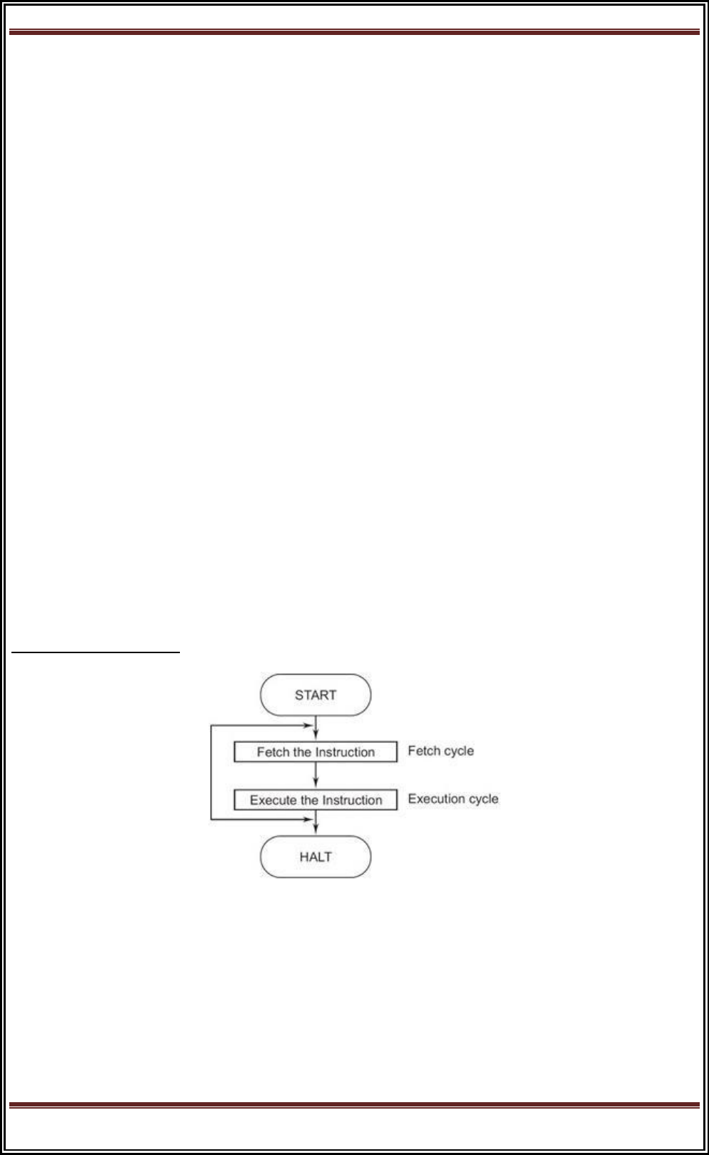
Instruction Cycle
In this chapter, we examine the sequences of micro operations that the Basic
Computer goes through for each instruction. Here, you should begin to understand
how the required control signals for each state of the CPU are determined, and how
they are generated by the control unit.
The CPU performs a sequence of micro operations for each instruction. The sequence
for each instruction of the Basic Computer can be refined into 4 abstract phases:
1. Fetch instruction
2. Decode
3. Fetch operand
4. Execute
Program execution can be represented as a top-down design:
1. Program execution
a. Instruction 1
i. Fetch instruction
ii. Decode
iii. Fetch operand
iv. Execute
b. Instruction 2
i. Fetch instruction
ii. Decode
iii. Fetch operand
iv. Execute
c. Instruction 3 ...

Computer Organization and Architecture
Page 58
Program execution begins with:
PC ← address of first instruction, SC ← 0
After this, the SC is incremented at each clock cycle until an instruction is completed,
and then it is cleared to begin the next instruction. This process repeats until a HLT
instruction is executed, or until the power is shut off.
Instruction Fetch and Decode
The instruction fetch and decode phases are the same for all instructions, so the
control functions and micro operations will be independent of the instruction code.
Everything that happens in this phase is driven entirely by timing variables T
0
, T
1
and
T
2
. Hence, all control inputs in the CPU during fetch and decode are functions of these
three variables alone.
T
0
: AR ← PC
T
1
: IR ← M[AR], PC ← PC + 1
T
2
: D
0-7
← decoded IR(12-14), AR ← IR(0-11), I ← IR(15)
For every timing cycle, we assume SC ← SC + 1 unless it is stated that SC ← 0.
The operation D
0-7
← decoded IR(12-14) is not a register transfer like most of our
micro operations, but is actually an inevitable consequence of loading a value into the
IR register. Since the IR outputs 12-14 are directly connected to a decoder, the outputs
of that decoder will change as soon as the new values of IR(12-14) propagate through
the decoder.
Note that incrementing the PC at time T
1
assumes that the next instruction is at
the next address. This may not be the case if the current instruction is a branch
instruction. However, performing the increment here will save time if the next
instruction immediately follows, and will do no harm if it doesn't. The incremented PC
value is simply overwritten by branch instructions.
In hardware development, unlike serial software development, it is often
advantageous to perform work that may not be necessary. Since we can perform
multiple micro operations at the same time, we might was well do everything
that might be useful at the earliest possible time. Likewise, loading AR with the

Computer Organization and Architecture
Page 59
address field from IR at T
2
is only useful if the instruction is a memory-reference
instruction. We won't know this until T
3
, but there is no reason to wait since there is
no harm in loading AR immediately.
Input-Output and Interrupt
Hardware Summary
The Basic Computer I/O consists of a simple terminal with a keyboard and a
printer/monitor.
The keyboard is connected serially (1 data wire) to the INPR register. INPR is a shift
register capable of shifting in external data from the keyboard one bit at a time. INPR
outputs are connected in parallel to the ALU.
Shift enable
|
v
+-----------+ 1 +-------+
| Keyboard |---/-->| INPR <|--- serial I/O clock
+-----------+ +-------+
|
/ 8
| | |
v v v
+---------------+
| ALU |
+---------------+
|
/ 16
|
v
+---------------+
| AC <|--- CPU master clock
+---------------+

Computer Organization and Architecture
Page 60
How many CPU clock cycles are needed to transfer a character from the keyboard to
the INPR register? (tricky)
Are the clock pulses provided by the CPU master clock?
RS232, USB, Firewire are serial interfaces with their own clock independent of the
CPU. ( USB speed is independent of processor speed. )
RS232: 115,200 kbps (some faster)
USB: 11 mbps
USB2: 480 mbps
FW400: 400 mbps
FW800: 800 mbps
USB3: 4.8 gbps
OUTR inputs are connected to the bus in parallel, and the output is connected serially
to the terminal. OUTR is another shift register, and the printer/monitor receives an
end-bit during each clock pulse.
I/O Operations
Since input and output devices are not under the full control of the CPU (I/O events
are asynchronous), the CPU must somehow be told when an input device has new
input ready to send, and an output device is ready to receive more output. The FGI flip-
flop is set to 1 after a new character is shifted into INPR. This is done by the I/O
interface, not by the control unit. This is an example of an asynchronous input event
(not synchronized with or controlled by the CPU).
The FGI flip-flop must be cleared after transferring the INPR to AC. This must be
done as a micro operation controlled by the CU, so we must include it in the CU design.
The FGO flip-flop is set to 1 by the I/O interface after the terminal has finished
displaying the last character sent. It must be cleared by the CPU after transferring a
character into OUTR. Since the keyboard controller only sets FGI and the CPU only
clears it, a JK flip-flop is convenient:
+-------+
Keyboard controller --->| J Q |----->
| | |

Computer Organization and Architecture
Page 61
+--------\-----\ | |
) or >----->|> FGI |
+--------/-----/ | |
| | |
CPU-------------------->| K |
+-------
How do we control the CK input on the FGI flip-flop? (Assume leading-edge
triggering.)
There are two common methods for detecting when I/O devices are ready,
namely software polling and interrupts. These two methods are discussed in the
following sections.
Stack Organization
Stack is the storage method of the items in which the last item included is the first one
to be removed/taken from the stack. Generally a stack in the computer is
a memory unit with an address register and the register holding the address of the
stack is known as the Stack Pointer (SP). A stack performs Insertion and Deletion
operation, were the operation of inserting an item is known as Push and operation of
deleting an item is known as Pop. Both Push and Pop operation results in
incrementing and decrementing the stack pointer respectively.
Register Stack
Register or memory words can be organized to form a stack. The stack pointer is
a register that holds the memory address of the top of the stack. When an item need
to be deleted from the stack, item on the top of the stack is deleted and the stack
pointer is decremented. Similarly, when an item needs to be added, the stack pointer is
incremented and writing the word at the position indicated by the stack pointer. There
are two 1 bit register; FULL and EMTY that are used for describing the
stack overflow and underflow conditions. Following micro-operations are performed
during inserting and deleting an item in/from the stack.
Insert:
SP <- SP + 1 // Increment the stack pointer to point the next higher address//

Computer Organization and Architecture
Page 62
M[SP] <- DR // Write the item on the top of the stack//
If (SP = 0) then (Full <- 1) // Check overflow condition //
EMTY <- 0 // Mark that the stack is not empty //
Delete:
DR <- M[SP] //Read an item from the top of the stack//
SP <- SP 1 //Decrement the stack pointer //
If (SP = 0) then (EMTY <- 1) //Check underflow condition //
FULL <- 0 //Mark that the stack is not full //
Get all the resource regarding the homework help and assignment help at
Transtutors.com. With our team of experts, we are capable of providing homework
help and assignment help for all levels. With us you can be rest assured the all the
content provided for homework help and assignment help will be original and
plagiarism free.
Register Stack:-
A stack can be placed in a portion of a large memory as it can be organized as a
collection of a finite number of memory words as register.

Computer Organization and Architecture
Page 63
In a 64- word stack, the stack pointer contains 6 bits because 26 = 64.
The one bit register FULL is set to 1 when the stack is full, and the one-bit register
EMTY is set to 1 when the stack is empty. DR is the data register that holes the binary
data to be written into on read out of the stack. Initially, SP is decide to O, EMTY is set
to 1, FULL = 0, so that SP points to the word at address O and the stack is masked
empty and not full.
PUSH SP ® SP + 1 increment stack pointer
M [SP] ® DR unit item on top of the Stack
It (SP = 0) then (FULL ® 1) check it stack is full
EMTY ® 0 mask the stack not empty.
POP DR ® [SP] read item trans the top of stack
SP ® SP –1 decrement SP
It (SP = 0) then (EMTY ® 1) check it stack is empty
FULL ® 0 mark the stack not full.
A stack can be placed in a portion of a large memory or it can be organized as
a collection of a finite number of memory words or registers. Figure X shows the
organization of a 64-word register stack. The stack pointer register SP contains a
binary number whose value is equal to the address of the word that is currently on
top of the stack.
Three items are placed in the stack: A, B, and C in the order. item C is
on the top of the stack so that the content of sp is now 3. To remove the top item, the
stack is popped by reading the memory word at address 3 and decrementing the
content of SP. Item B is now on top of the stack since SP holds address 2. To insert a
new item, the stack is pushed by incrementing SP and writing a word in the next
higher location in the stack. Note that item C has read out but not physically removed.
This does not matter because when the stack is pushed, a new item is written in its
place.
In a 64-word stack, the stack pointer contains 6 bits because 26=64. since SP
has only six bits, it cannot exceed a number greater than 63(111111 in binary). When

Computer Organization and Architecture
Page 64
63 is incremented by 1, the result is 0 since 111111 + 1 =1000000 in binary, but SP
can accommodate only the six least significant bits. Similarly, when 000000 is
decremented by 1, the result is 111111. The one bit register Full is set to 1 when the
stack is full, and the one-bit register EMTY is set to 1 when the stack is empty of
items. DR is the data register that holds the binary data to be written in to or read out
of the stack.
Initially, SP is cleared to 0, Emty is set to 1, and Full is cleared to 0, so that SP
points to the word at address o and the stack is marked empty and not full. if the stack
is not full , a new item is inserted with a push operation. the push operation is
implemented with the following sequence of micro-operation.
SP ←SP + 1 (Increment stack pointer)
M(SP) ← DR (Write item on top of the stack)
if (sp=0) then (Full ← 1) (Check if stack is full)
Emty ← 0 ( Marked the stack not empty)
The stack pointer is incremented so that it points to the address of the next-higher
word. A memory write operation inserts the word from DR into the top of the stack.
Note that SP holds the address of the top of the stack and that M(SP) denotes the
memory word specified by the address presently available in SP, the first item stored
in the stack is at address 1. The last item is stored at address 0, if SP reaches 0, the
stack is full of item, so FULLL is set to 1.
This condition is reached if the top item prior to the last push was in location 63
and after increment SP, the last item stored in location 0. Once an item is stored in
location 0, there are no more empty register in the stack. If an item is written in the
stack, obviously the stack cannot be empty, so EMTY is cleared to 0.
DR← M[SP] Read item from the top of stack
SP ← SP-1 Decrement stack Pointer
if( SP=0) then (Emty ← 1) Check if stack is empty
FULL ← 0 Mark the stack not full

Computer Organization and Architecture
Page 65
The top item is read from the stack into DR. The stack pointer is then decremented. if
its value reaches zero, the stack is empty, so Empty is set to 1. This condition is
reached if the item read was in location 1. Once this item is read out, SP is
decremented and reaches the value 0, which is the initial value of SP. Note that if a
pop operation reads the item from location 0 and then SP is decremented, SP changes
to 111111, which is equal to decimal 63. In this configuration, the word in address 0
receives the last item in the stack. Note also that an erroneous operation will result if
the stack is pushed when FULL=1 or popped when EMTY =1.
Memory Stack :
A stack can exist as a stand-alone unit as in figure 4 or can be implemented in
a random access memory attached to CPU. The implementation of a stack in the CPU
is done by assigning a portion of memory to a stack operation and using a processor
register as a stack pointer. Figure shows a portion of computer memory partitioned in
to three segment program, data and stack. The program counter PC points at the
address of the next instruction in the program. The address register AR points at an
array of data. The stack pointer SP points at the top of the stack. The three register
are connected to a common address bus, and either one can provide an address for
memory. PC is used during the fetch phase to read an instruction. AR is used during
the execute phase to read an operand. SP is used to push or POP items into or from
the stack.
As show in figure :4 the initial value of SP is 4001 and the stack grows with
decreasing addresses. Thus the first item stored in the stack is at address 4000, the
second item is stored at address 3999, and the last address hat can be used for the
stack is 3000. No previous are available for stack limit checks.
We assume that the items in the stack communicate with a data register DR. A new
item is inserted with the push operation as follows.
SP← SP-1
M[SP] ← DR

Computer Organization and Architecture
Page 66
The stack pointer is decremented so that it points at the address of the next word. A
Memory write operation insertion the word from DR into the top of the stack. A new
item is deleted with a pop operation as follows.
DR← M[SP]
SP←SP + 1
The top item is read from the stack in to DR. The stack pointer is then incremented to
point at the next item in the stack. Most computers do not provide hardware to check
for stack overflow (FULL) or underflow (Empty). The stack limit can be checked by
using two processor register: one to hold upper limit and other hold the lower limit.
After the pop or push operation SP is compared with lower or upper limit register.
REVERSE POLISH NOTATION
For example: A x B + C x D is an arithmetical expression written in infix notation, here
x (denotes multiplication). In this expression A and B are two operands and x is an
operator, similarly C and D are two operands and x is an operator. In this expression +

Computer Organization and Architecture
Page 67
is another operator which is written between (A x B) and (C x D). Because of the
precedence of the operator multiplication is done first. The order of precedence is as:
1. Exponentiation have precedence one.
2. Multiplication and Division has precedence two.
3. Addition and subtraction has precedence three.
Reverse polish notation is also known as postfix notation is defined as: In postfix
notation operator is written after the operands. Examples of postfix notation are AB+
and CD-. Here A and B are two operands and the operator is written after these two
operands. The conversion from infix expression into postfix expression is shown
below.
Convert the infix notation A x B + C x D + E x F into postfix notation?
SOLUTION
A x B + C x D + E x F
= [ABx] + [CDx] + [EFx]
= [ABxCDx] + [EFx]
= [ABxCDxEFx]
= ABxCDxEFx
So the postfix notation is ABxCDxEFx.
Convert the infix notation {A – B + C x (D x E – F)} / G + H x K into postfix
notation?
{A – B + C x (D x E – F)} / G + H x K
= {A – B + C x ([DEx] – F)} / G + [HKx]
= {A – B + C x [DExF-]} / [GHKx+]
= {A – B + [CDExF-x]} / [GHKx+]
= {[AB-] + [CDExF-x]} / [GHKx+]
= [AB-CDExF-x+] / [GHKx+]
= [AB-CDExF-x+GHKx+/]
= AB-CDExF-x+GHKx+/
So the postfix notation is AB-CDExF-x+GHKx+/.
Now let’s how to evaluate a postfix expression, the algorithm for the evaluation of
postfix notation is shown below:

Computer Organization and Architecture
Page 68
ALGORITHM:
(Evaluation of Postfix notation) This algorithm finds the result of a postfix expression.
Step1: Insert a symbol (say #) at the right end of the postfix expression.
Step2: Scan the expression from left to right and follow the Step3 and Step4 for each of
the symbol encountered.
Step3: if an element is encountered insert into stack.
Step4: if an operator (say &) is encountered pop the top element A (say) and next to
top element B (say) perform the following operation x = B&A. Push x into the top of
the stack.
Step5: if the symbol # is encountered then stop scanning.
Evaluate the post fix expression 50 4 3 x 2 – + 7 8 x 4 / -?
SOLUTION
Put symbol # at the right end of the expression: 50 4 3 x 2 – + 7 8 x 4 / – #.
Postfix expression
Symbol
scanned
Stack
50 4 3 x 2 – + 7 8 x 4 / – #
_
_
4 3 x 2 – + 7 8 x 4 / – #
50
50
3 x 2 – + 7 8 x 4 / – #
4
50, 4
x 2 – + 7 8 x 4 / – #
3
50, 4, 3
2 – + 7 8 x 4 / – #
x
50, 12
– + 7 8 x 4 / – #
2
50, 12, 2
+ 7 8 x 4 / – #
–
50, 10
7 8 x 4 / – #
+
60
8 x 4 / – #
7
60, 7
x 4 / – #
8
60, 7, 8
4 / – #
x
60, 56
/ – #
4
60, 56, 4
– #
/
60, 14

Computer Organization and Architecture
Page 69
#
–
46
_
#
Result = 46
INSTRUCTION FORMATS
The most common fields found in instruction format are:-
(1) An operation code field that specified the operation to be performed
(2) An address field that designates a memory address or a processor registers.
(3) A mode field that specifies the way the operand or the effective address is
determined.
Computers may have instructions of several different lengths containing varying
number of addresses. The number of address field in the instruction format of a
computer depends on the internal organization of its registers. Most computers fall
into one of three types of CPU organization.
(1) Single Accumulator organization ADD X AC ® AC + M [×]
(2) General Register Organization ADD R1, R2, R3 R ® R2 + R3
(3) Stack Organization PUSH X
Three address Instruction
Computer with three addresses instruction format can use each address field to
specify either processor register are memory operand.
ADD R1, A, B A1 ® M [A] + M [B]
ADD R2, C, D R2 ® M [C] + M [B] X = (A + B) * (C + A)
MUL X, R1, R2 M [X] R1 * R2
The advantage of the three address formats is that it results in short program when
evaluating arithmetic expression. The disadvantage is that the binary-coded
instructions require too many bits to specify three addresses.
Two Address Instruction

Computer Organization and Architecture
Page 70
Most common in commercial computers. Each address field can specify either a
processes register on a memory word.
MOV R1, A R1 ® M [A]
ADD R1, B R1 ® R1 + M [B]
MOV R2, C R2 ® M [C] X = (A + B) * ( C + D)
ADD R2, D R2 ® R2 + M [D]
MUL R1, R2 R1 ® R1 * R2
MOV X1 R1 M [X] ® R1
One Address instruction
It used an implied accumulator (AC) register for all data manipulation. For
multiplication/division, there is a need for a second register.
LOAD A AC ® M [A]
ADD B AC ® AC + M [B]
STORE T M [T] ® AC X = (A +B) × (C + A)
All operations are done between the AC register and a memory operand. It’s the
address of a temporary memory location required for storing the intermediate result.
LOAD C AC ® M (C)
ADD D AC ® AC + M (D)
ML T AC ® AC + M (T)
STORE X M [×]® AC
Zero – Address Instruction
A stack organized computer does not use an address field for the instruction ADD and
MUL. The PUSH & POP instruction, however, need an address field to specify the
operand that communicates with the stack (TOS ® top of the stack)
PUSH A TOS ® A
PUSH B TOS ® B
ADD TOS ® (A + B)
PUSH C TOS ® C
PUSH D TOS ® D
ADD TOS ® (C + D)

Computer Organization and Architecture
Page 71
MUL TOS ® (C + D) * (A + B)
POP X M [X] TOS
Addressing Modes
The operation field of an instruction specifies the operation to be performed. This
operation must be executed on some data stored in computer register as memory
words. The way the operands are chosen during program execution is dependent on
the addressing mode of the instruction. The addressing mode specifies a rule for
interpreting or modifying the address field of the instruction between the operand is
activity referenced. Computer use addressing mode technique for the purpose of
accommodating one or both of the following provisions.
(1) To give programming versatility to the uses by providing such facilities as
pointer to memory, counters for top control, indexing of data, and program relocation.
(2) To reduce the number of bits in the addressing fields of the instruction.
Addressing Modes: The most common addressing techniques are
• Immediate
• Direct
• Indirect
• Register
• Register Indirect
• Displacement
• Stack
All computer architectures provide more than one of these addressing modes.
The question arises as to how the control unit can determine which addressing mode
is being used in a particular instruction. Several approaches are used. Often, different
opcodes will use different addressing modes. Also, one or more bits in the instruction

Computer Organization and Architecture
Page 72
format can be used as a mode field. The value of the mode field determines which
addressing mode is to be used.
What is the interpretation of effective address. In a system without virtual
memory, the effective address will be either a main memory address or a register. In a
virtual memory system, the effective address is a virtual address or a register. The
actual mapping to a physical address is a function of the paging mechanism and is
invisible to the programmer.
Opcode
Mode
Address
Immediate Addressing:
The simplest form of addressing is immediate addressing, in which the
operand is actually present in the instruction:
OPERAND = A
This mode can be used to define and use constants or set initial values of
variables. The advantage of immediate addressing is that no memory reference other
than the instruction fetch is required to obtain the operand. The disadvantage is that
the size of the number is restricted to the size of the address field, which, in most
instruction sets, is small compared with the world length.
Direct Addressing:
A very simple form of addressing is direct addressing, in which the address field
contains the effective address of the operand:

Computer Organization and Architecture
Page 73
EA = A
It requires only one memory reference and no special calculation.
Indirect Addressing:
With direct addressing, the length of the address field is usually less than the
word length, thus limiting the address range. One solution is to have the address field
refer to the address of a word in memory, which in turn contains a full-length address
of the operand. This is known as indirect addressing:
EA = (A)
Register Addressing:
Register addressing is similar to direct addressing. The only difference is that
the address field refers to a register rather than a main memory address:
EA = R

Computer Organization and Architecture
Page 74
The advantages of register addressing are that only a small address field is
needed in the instruction and no memory reference is required. The disadvantage of
register addressing is that the address space is very limited.
The exact register location of the operand in case of Register Addressing
Mode is shown in the Figure 34.4. Here, 'R' indicates a register where the operand is
present.
Register Indirect Addressing:
Register indirect addressing is similar to indirect addressing, except that the
address field refers to a register instead of a memory location. It requires only one
memory reference and no special calculation.
EA = (R)
Register indirect addressing uses one less memory reference than indirect
addressing. Because, the first information is available in a register which is nothing
but a memory address. From that memory location, we use to get the data or
information. In general, register access is much more faster than the memory access.
Displacement Addressing:

Computer Organization and Architecture
Page 75
A very powerful mode of addressing combines the capabilities of direct
addressing and register indirect addressing, which is broadly categorized as
displacement addressing:
EA = A + (R)
Displacement addressing requires that the instruction have two address fields,
at least one of which is explicit. The value contained in one address field (value = A)
is used directly. The other address field, or an implicit reference based on opcode,
refers to a register whose contents are added to A to produce the effective address.
The general format of Displacement Addressing is shown in the Figure 4.6.
Three of the most common use of displacement addressing are:
• Relative addressing
• Base-register addressing
• Indexing
Relative Addressing:
For relative addressing, the implicitly referenced register is the program
counter (PC). That is, the current instruction address is added to the address field to
produce the EA. Thus, the effective address is a displacement relative to the address
of the instruction.
Base-Register Addressing:

Computer Organization and Architecture
Page 76
The reference register contains a memory address, and the address field
contains a displacement from that address. The register reference may be explicit or
implicit. In some implementation, a single segment/base register is employed and is
used implicitly. In others, the programmer may choose a register to hold the base
address of a segment, and the instruction must reference it explicitly.
Indexing:
The address field references a main memory address, and the reference
register contains a positive displacement from that address. In this case also the
register reference is sometimes explicit and sometimes implicit.
Generally index register are used for iterative tasks, it is typical that there is a
need to increment or decrement the index register after each reference to it. Because
this is such a common operation, some system will automatically do this as part of the
same instruction cycle.
This is known as auto-indexing. We may get two types of auto-indexing: -one is
auto-incrementing and the other one is -auto-decrementing. If certain registers are
devoted exclusively to indexing, then auto-indexing can be invoked implicitly and
automatically. If general purpose register are used, the auto index operation may need
to be signaled by a bit in the instruction.
Auto-indexing using increment can be depicted as follows:
EA = A + (R)
R = (R) + 1
Auto-indexing using decrement can be depicted as follows:
EA = A + (R)
R = (R) - 1
In some machines, both indirect addressing and indexing are provided, and it is
possible to employ both in the same instruction. There are two possibilities: The
indexing is performed either before or after the indirection. If indexing is performed
after the indirection, it is termed post indexing
EA = (A) + (R)

Computer Organization and Architecture
Page 77
First, the contents of the address field are used to access a memory location
containing an address. This address is then indexed by the register value.
With pre indexing, the indexing is performed before the indirection:
EA = ( A + (R)
An address is calculated, the calculated address contains not the operand, but the
address of the operand.
Stack Addressing:
A stack is a linear array or list of locations. It is sometimes referred to as a
pushdown list or last-in-first-out queue. A stack is a reserved block of locations. Items
are appended to the top of the stack so that, at any given time, the block is partially
filled. Associated with the stack is a pointer whose value is the address of the top of
the stack. The stack pointer is maintained in a register. Thus, references to stack
locations in memory are in fact register indirect addresses.
The stack mode of addressing is a form of implied addressing. The machine
instructions need not include a memory reference but implicitly operate on the top of
the stack.
Value addition: A Quick View
Various Addressing Modes with Examples
The most common names for addressing modes (names may differ
among architectures)
Addressing
modes
Example
Instruction
Meaning
When used
Register
Add R4,R3
R4 <- R4 + R3
When a value is
in a register
Immediate
Add R4, #3
R4 <- R4 + 3
For constants
Displacement
Add R4,
100(R1)
R4 <- R4 +
Mem[100+R1]
Accessing local
variables
Register
deffered
Add R4,(R1)
R4 <- R4 + M[R1]
Accessing using
a pointer or a
computed
address
Indexed
Add R3, (R1
+ R2)
R3 <- R3 +
Mem[R1+R2]
Useful in array
addressing:
R1 - base of
array
R2 - index
amount

Computer Organization and Architecture
Page 78
Direct
Add R1,
(1001)
R1 <- R1 + Mem[1001]
Useful in
accessing static
data
Memory
deferred
Add R1,
@(R3)
R1 <- R1 +
Mem[Mem[R3]]
If R3 is the
address of a
pointer p, then
mode yields *p
Auto-
increment
Add R1,
(R2)+
R1 <- R1 +Mem[R2]
R2 <- R2 + d
Useful for
stepping
through arrays
in a loop.
R2 - start of
array
d - size of an
element
Auto-
decrement
Add R1,-
(R2)
R2 <-R2-d
R1 <- R1 + Mem[R2]
Same as
autoincrement.
Both can also
be used to
implement a
stack as push
and pop
Scaled
Add R1,
100(R2)[R3]
R1<-
R1+Mem[100+R2+R3*d]
Used to index
arrays. May be
applied to any
base
addressing
mode in some
machines.
Notation:
<- - assignment
Mem - the name for memory:
Mem[R1] refers to contents of memory location whose address is given by the
contents of R1
Source: Self
Data Transfer & Manipulation
Computer provides an extensive set of instructions to give the user the flexibility to
carryout various computational task. Most computer instruction can be classified into
three categories.
(1) Data transfer instruction
(2) Data manipulation instruction
(3) Program control instruction
Data transfer instruction cause transferred data from one location to another without
changing the binary instruction content. Data manipulation instructions are those that
perform arithmetic logic, and shift operations. Program control instructions provide
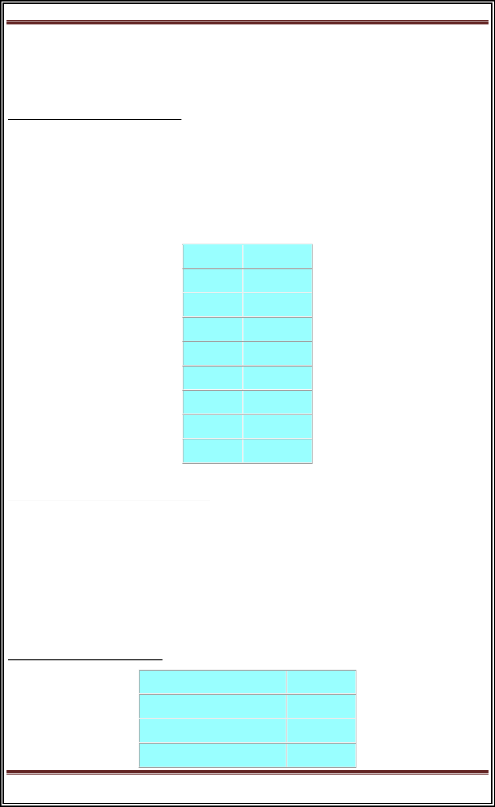
Computer Organization and Architecture
Page 79
decision-making capabilities and change the path taken by the program when
executed in the computer.
(1) Data Transfer Instruction
Data transfer instruction move data from one place in the computer to another
without changing the data content. The most common transfers are between memory
and processes registers, between processes register & input or output, and between
processes register themselves
(Typical data transfer instruction)
Name
Mnemonic
Load
LD
Store
ST
Move
MOV
Exchange
XCH
Input
IN
Output
OUT
Push
PUSH
Pop
POP
(2) Data Manipulation Instruction
It performs operations on data and provides the computational capabilities for the
computer. The data manipulation instructions in a typical computer are usually
divided into three basic types.
(a) Arithmetic Instruction
(b) Logical bit manipulation Instruction
(c) Shift Instruction.
(a) Arithmetic Instruction
Name
Mnemonic
Increment
INC
Decrement
DEC
Add
Add

Computer Organization and Architecture
Page 80
Subtract
Sub
Multiply
MUL
Divide
DIV
Add with Carry
ADDC
Subtract with Basses
SUBB
Negate (2’s Complement)
NEG
(b) Logical & Bit Manipulation Instruction
Name
Mnemonic
Clear
CLR
Complement
COM
AND
AND
OR
OR
Exclusive-Or
XOR
Clear Carry
CLRC
Set Carry
SETC
Complement Carry
COMC
Enable Interrupt
ET
Disable Interrupt
OI
(c) Shift Instruction
Instructions to shift the content of an operand are quite useful and one often provided
in several variations. Shifts are operation in which the bits of a word are moved to the
left or right. The bit-shifted in at the and of the word determines the type of shift used.
Shift instruction may specify either logical shift, arithmetic shifts, or rotate type shifts.
Name
Mnemonic
Logical Shift right
SHR
Logical Shift left
SHL
Arithmetic shift right
SHRA
Arithmetic shift left
SHLA
Rotate right
ROR

Computer Organization and Architecture
Page 81
Rotate left
ROL
Rotate right through carry
RORC
Rotate left through carry
ROLC
Introduction About Program Control:-
A program that enhances an operating system by creating an environment in which
you can run other programs. Control programs generally provide a graphical
interface and enable you to run several programs at once in different windows.
Control programs are also called operating environments.
The program control functions are used when a series of conditional or
unconditional jump and return instruction are required. These instructions allow the
program to execute only certain sections of the control logic if a fixed set of logic
conditions are met. The most common instructions for the program control available
in most controllers are described in this section.
Introduction About status bit register:-
A status register, flag register, or condition code register is a collection of
status flag bits for a processor. An example is the FLAGS register of the computer
architecture. The flags might be part of a larger register, such as a program status
word (PSW) register.
The status register is a hardware register which contains information about the
state of the processor. Individual bits are implicitly or explicitly read and/or written
by the machine code instructions executing on the processor. The status register in a
traditional processor design includes at least three central flags: Zero, Carry, and
Overflow, which are set or cleared automatically as effects of arithmetic and bit
manipulation operations. One or more of the flags may then be read by a subsequent
conditional jump instruction (including conditional calls, returns, etc. in some
machines) or by some arithmetic, shift/rotate or bitwise operation, typically using the
carry flag as input in addition to any explicitly given operands. There are also
processors where other classes of instructions may read or write the fundamental

Computer Organization and Architecture
Page 82
zero, carry or overflow flags, such as block-, string- or dedicated input/output
instructions, for instance.
Some CPU architectures, such as the MIPS and Alpha, do not use a dedicated flag
register. Others do not implicitly set and/or read flags. Such machines either do not
pass implicit status information between instructions at all, or do they pass it in a
explicitly selected general purpose register.
A status register may often have other fields as well, such as more specialized
flags, interrupt enable bits, and similar types of information. During an interrupt, the
status of the thread currently executing can be preserved (and later recalled) by
storing the current value of the status register along with the program counter and
other active registers into the machine stack or some other reserved area of memory.
Common flags:-
This is a list of the most common CPU status register flags, implemented in almost all
modern processors.
Flag
Name
Description
Z
Zero flag
Indicates that the result of arithmetic or logical
operation (or, sometimes, a load) was zero.
C
Carry flag
Enables numbers larger than a single word to be
added/subtracted by carrying a binary digit from a less
significant word to the least significant bit of a more
significant word as needed. It is also used to extend bit
shifts and rotates in a similar manner on many
processors (sometimes done via a dedicated X flag).
S / N
Sign flag
Negative
flag
Indicates that the result of a mathematical operation is
negative. In some processors, the N and S flags are
distinct with different meanings and usage: One
indicates whether the last result was negative whereas
the other indicates whether a subtraction or addition
has taken place.

Computer Organization and Architecture
Page 83
V / O / W
Overflow
flag
Indicates that the signed result of an operation is too
large to fit in the register width using twos complement
representation.
Introduction About Conditional branch instruction:-
Conditional branch instruction:-
Conditional branch instruction is the branch instruction bit and BR instruction is the
Program control instruction.
The conditional Branch Instructions are listed as Bellow:-
Mnemonics
Branch Instruction
Tested control
BZ
Branch if Zero
Z=1
BNZ
Branch if not Zero
Z=0
BC
Branch if Carry
C=1
BNC
Branch if not Carry
C=0
BP
Branch if Plus
S=0
BM
Branch if Minus
S=1
BV
Branch if Overflow
V=1
BNV
Branch if not Overflow
V=0
Unsigned Compare(A-B):-
Mnemonics
Branch Instruction
Tested control
BHI
Branch if Higher
A > B
BHE
Branch if Higher or Equal
A >= B
BLO
Branch if Lower
A < B
BLE
Branch if Lower or Equal
A <= B
BE
Branch if Equal
A=B
BNE
Branch if not Equal
A not = B
Signed Compare(A-B):
Mnemonics
Branch Instruction
Tested control

Computer Organization and Architecture
Page 84
BGT
Branch if Greater Than
A > B
BGE
Branch if Greater Than or Equal
A >= B
BLT
Branch if Less Than
A < B
BLE
Branch if Less Than or Equal
A <= B
BE
Branch if Equal
A=B
BNE
Branch if not Equal
A not = B
Introduction About program interrupt:-
When a Process is executed by the CPU and when a user Request for another Process
then this will create disturbance for the Running Process. This is also called as
the Interrupt.
Interrupts can be generated by User, Some Error Conditions and also by
Software’s and the hardware’s. But CPU will handle all the Interrupts very carefully
because when Interrupts are generated then the CPU must handle all the Interrupts
Very carefully means the CPU will also Provide Response to the Various Interrupts
those are generated. So that When an interrupt has Occurred then the CPU will handle
by using the Fetch, decode and Execute Operations.
Interrupts allow the operating system to take notice of an external event, such
as a mouse click. Software interrupts, better known as exceptions, allow the OS to
handle unusual events like divide-by-zero errors coming from code execution.
The sequence of events is usually like this:
Hardware signals an interrupt to the processor
The processor notices the interrupt and suspends the currently running software
The processor jumps to the matching interrupt handler function in the OS
The interrupt handler runs its course and returns from the interrupt
The processor resumes where it left off in the previously running software
The most important interrupt for the operating system is the timer tick interrupt. The
timer tic interrupt allows the OS to periodically regain control from the currently
running user process. The OS can then decide to schedule another process, return back

Computer Organization and Architecture
Page 85
to the same process, do housekeeping, etc. The timer tick interrupt provides the
foundation for the concept of preemptive multitasking.
TYPES OF INTERRUPTS
Generally there are three types of Interrupts those are Occurred For Example
1) Internal Interrupt
2) External Interrupt.
3) Software Interrupt.
1.Internal Interrupt:
• When the hardware detects that the program is doing something wrong, it will
usually generate an interrupt usually generate an interrupt.
– Arithmetic error - Invalid Instruction
– Addressing error - Hardware malfunction
– Page fault – Debugging
• A Page Fault interrupt is not the result of a program error, but it does require the
operating system to get control.
The Internal Interrupts are those which are occurred due to Some Problem in
the Execution For Example When a user performing any Operation which contains any
Error and which contains any type of Error. So that Internal Interrupts are those
which are occurred by the Some Operations or by Some Instructions and the
Operations those are not Possible but a user is trying for that Operation. And The
Software Interrupts are those which are made some call to the System for Example
while we are Processing Some Instructions and when we wants to Execute one more
Application Programs.
2.External Interrupt:
• I/O devices tell the CPU that an I/O request has completed by sending an interrupt
signal to the processor.
• I/O errors may also generate an interrupt.

Computer Organization and Architecture
Page 86
• Most computers have a timer which interrupts the CPU every so many interrupts the
CPU every so many milliseconds.
The External Interrupt occurs when any Input and Output Device request for any
Operation and the CPU will Execute that instructions first For Example When a
Program is executed and when we move the Mouse on the Screen then the CPU will
handle this External interrupt first and after that he will resume with his Operation.
3.Software interrupts:
These types if interrupts can occur only during the execution of an instruction. They
can be used by a programmer to cause interrupts if need be. The primary purpose of
such interrupts is to switch from user mode to supervisor mode.
A software interrupt occurs when the processor executes an INT instruction.
Written in the program, typically used to invoke a system service. A processor
interrupt is caused by an electrical signal on a processor pin. Typically used by devices
to tell a driver that they require attention. The clock tick interrupt is very common; it
wakes up the processor from a halt state and allows the scheduler to pick other work
to perform.
A processor fault like access violation is triggered by the processor itself when it
encounters a condition that prevents it from executing code. Typically when it tries to
read or write from unmapped memory or encounters an invalid instruction.
CISC Characteristics
A computer with large number of instructions is called complex instruction set
computer or CISC. Complex instruction set computer is mostly used in scientific
computing applications requiring lots of floating point arithmetic.
A large number of instructions - typically from 100 to 250 instructions.
Some instructions that perform specialized tasks and are used infrequently.
A large variety of addressing modes - typically 5 to 20 different modes.
Variable-length instruction formats

Computer Organization and Architecture
Page 87
Instructions that manipulate operands in memory.
RISC Characteristics
A computer with few instructions and simple construction is called reduced
instruction set computer or RISC. RISC architecture is simple and efficient. The major
characteristics of RISC architecture are,
Relatively few instructions
Relatively few addressing modes
Memory access limited to load and store instructions
All operations are done within the registers of the CPU
Fixed-length and easily-decoded instruction format.
Single cycle instruction execution
Hardwired and micro programmed control
Example of RISC & CISC
Examples of CISC instruction set architectures are PDP-11, VAX, Motorola 68k,
and your desktop PCs on intel’s x86 architecture based too .
Examples of RISC families include DEC Alpha, AMD 29k, ARC, Atmel AVR,
Blackfin, Intel i860 and i960, MIPS, Motorola 88000, PA-RISC, Power (including PowerPC),
SuperH, SPARC and ARM too.

Computer Organization and Architecture
Page 88
Which one is better ?
We cannot differentiate RISC and CISC technology because both are suitable at its specific
application. What counts is how fast a chip can execute the instructions it is given and how well it
runs existing software. Today, both RISC and CISC manufacturers are doing everything to get an
edge on the competition.
http://www.laureateiit.com/projects/bacii2014/projects/coa_anil/i_o_interface.html
UNIT – III (12 Lectures)
MICRO‐PROGRAMMED CONTROL: Control memory, address sequencing, micro‐program
example, design of control unit.
Book: M. Moris Mano (2006), Computer System Architecture, 3rd edition, Pearson/PHI,
India: Unit-7 Pages: 213-238

Computer Organization and Architecture
Page 89
COMPUTER ARITHMETIC: Addition and subtraction, multiplication and division algorithms,
floating‐point arithmetic operation, decimal arithmetic unit, decimal arithmetic operations.
Book: M. Moris Mano (2006), Computer System Architecture, 3rd edition, Pearson/PHI,
India: Unit-10 Pages: 333-380
Control Memory:
Control memory is a random access memory(RAM) consisting of addressable storage
registers. It is primarily used in mini and mainframe computers. It is used as a temporary
storage for data. Access to control memory data requires less time than to main memory; this
speeds up CPU operation by reducing the number of memory references for data storage and
retrieval. Access is performed as part of a control section sequence while the master clock
oscillator is running. The control memory addresses are divided into two groups: a task mode
and an executive (interrupt) mode.
Addressing words stored in control memory is via the address select logic for each of
the register groups. There can be up to five register groups in control memory. These groups
select a register for fetching data for programmed CPU operation or for maintenance console
or equivalent display or storage of data via maintenance console or equivalent. During
programmed CPU operations, these registers are accessed directly by the CPU logic. Data
routing circuits are used by control memory to interconnect the registers used in control
memory. Some of the registers contained in a control memory that operate in the task and
the executive modes include the following: Accumulators Indexes Monitor clock status
indicating registers Interrupt data registers
• The control unit in a digital computer initiates sequences of micro operations
• The complexity of the digital system is derived form the number of sequences that are
performed
• When the control signals are generated by hardware, it is hardwired
• In a bus-oriented system, the control signals that specify micro operations are groups of bits
that select the paths in multiplexers, decoders, and ALUs.

Computer Organization and Architecture
Page 90
• The control unit initiates a series of sequential steps of micro operations
• The control variables can be represented by a string of 1’s and 0’s called a control word
• A micro programmed control unit is a control unit whose binary control variables are stored
in memory
• A sequence of microinstructions constitutes a micro program
• The control memory can be a read-only memory
• Dynamic microprogramming permits a micro program to be loaded and uses a writable
control memory
• A computer with a micro programmed control unit will have two separate memories: a
main memory and a control memory
• The micro program consists of microinstructions that specify various internal control
signals for execution of register micro operations
• These microinstructions generate the micro operations to:
fetch the instruction from main memory
evaluate the effective address
execute the operation
return control to the fetch phase for the next instruction
• The control memory address register specifies the address of the microinstruction
• The control data register holds the microinstruction read from memory
• The microinstruction contains a control word that specifies one or more micro operations
for the data processor
• The location for the next micro instruction may, or may not be the next in sequence
• Some bits of the present micro instruction control the generation of the address of the next
micro instruction
• The next address may also be a function of external input conditions
• While the micro operations are being executed, the next address is computed in the next
address generator circuit (sequencer) and then transferred into the CAR to read the next
micro instructions
• Typical functions of a sequencer are: o incrementing the CAR by one
loading into the CAR and address from control memory
transferring an external address
loading an initial address to start the control operations

Computer Organization and Architecture
Page 91
• A clock is applied to the CAR and the control word and next-address information are taken
directly from the control memory
• The address value is the input for the ROM and the control work is the output
• No read signal is required for the ROM as in a RAM
• The main advantage of the micro programmed control is that once the
hardware configuration is established, there should be no need for h/w or wiring changes
• To establish a different control sequence, specify a different set of microinstructions for
control memory
Addressing Sequencing:
Each machine instruction is executed through the application of a sequence of
microinstructions. Clearly, we must be able to sequence these; the collection of
microinstructions which implements a particular machine instruction is called a routine.
The MCU typically determines the address of the first microinstruction which
implements a machine instruction based on that instruction's opcode. Upon machine power-
up, the CAR should contain the address of the first microinstruction to be executed.
The MCU must be able to execute microinstructions sequentially (e.g., within routines), but
must also be able to ``branch'' to other microinstructions as required; hence, the need for a
sequencer.
The microinstructions executed in sequence can be found sequentially in the CM, or
can be found by branching to another location within the CM. Sequential retrieval of
microinstructions can be done by simply incrementing the current CAR contents; branching
requires determining the desired CW address, and loading that into the CAR.
CAR
Control Address Register

Computer Organization and Architecture
Page 92
control ROM
control memory (CM); holds CWs
opcode
opcode field from machine instruction
mapping logic
hardware which maps opcode into microinstruction address
branch logic
determines how the next CAR value will be determined from all the various possibilities
multiplexors
implements choice of branch logic for next CAR value
incrementer
generates CAR + 1 as a possible next CAR value
SBR
used to hold return address for subroutine-call branch operations
Conditional branches are necessary in the micro program. We must be able to perform
some sequences of micro-ops only when certain situations or conditions exist (e.g., for
conditional branching at the machine instruction level); to implement these, we need to be
able to conditional execute or avoid certain microinstructions within routines.
Subroutine branches are helpful to have at the micro program level. Many routines
contain identical sequences of microinstructions; putting them into subroutines allows those
routines to be shorter, thus saving memory. Mapping of opcodes to microinstruction
addresses can be done very simply. When the CM is designed, a ``required'' length is
determine for the machine instruction routines (i.e., the length of the longest one). This is
rounded up to the next power of 2, yielding a value k such that 2 k microinstructions will be
sufficient to implement any routine.
The first instruction of each routine will be located in the CM at multiples of this
``required'' length. Say this is N. The first routine is at 0; the next, at N; the next, at 2*N; etc.
This can be accomplished very easily. For instance, with a four-bit opcode and routine length
of four microinstructions, k is two; generate the microinstruction address by appending two
zero bits to the opcode:

Computer Organization and Architecture
Page 93
Alternately, the n-bit opcode value can be used as the ``address'' input of a 2n x M ROM; the
contents of the selected ``word'' in the ROM will be the desired M-bit CAR address for the
beginning of the routine implementing that instruction. (This technique allows for variable-
length routines in the CM.) >pp We choose between all the possible ways of generating CAR
values by feeding them all into a multiplexor bank, and implementing special branch logic
which will determine how the muxes will pass on the next address to the CAR.
As there are four possible ways of determining the next address, the multiplexor bank
is made up of N 4x1 muxes, where N is the number of bits in the address of a CW. The branch
logic is used to determine which of the four possible ``next address'' values is to be passed on
to the CAR; its two output lines are the select inputs for the muxes.

Computer Organization and Architecture
Page 94
Addition and Subtraction
Four basic computer arithmetic operations are addition, subtraction, division and
multiplication. The arithmetic operation in the digital computer manipulate data to produce
results. It is necessary to design arithmetic procedures and circuits to program arithmetic
operations using algorithm. The algorithm is a solution to any problem and it is stated by a
finite number of well-defined procedural steps. The algorithms can be developed for the
following types of data.
1. Fixed point binary data in signed magnitude representation
2. Fixed point binary data in signed 2’s complement representation.
3. Floating point representation
4. Binary Coded Decimal (BCD) data
Addition and Subtraction with signed magnitude
Consider two numbers having magnitude A and B. When the signed numbers are added or
subtracted, there can be 8 different conditions depending on the sign and the operation
performed as shown in the table below:
Operation
Add magnitude
When A > B
When A < B
When A = B
(+A) + (+B)
+(A + B)
--
--
--
(+A) + (-B)
--
+(A - B)
-(B - A)
+(A - B)
(-A) + (+B)
--
-(A - B)
+(B - A)
+(A - B)
(-A) + (-B)
-(A + B)
--
--
--
(+A) - (+B)
--
+(A - B)
-(B - A)
+(A - B)
(+A) - (-B)
+(A + B)
--
--
--
(-A) - (+B)
-(A + B)
--
--
--
(-A) - (-B)
--
-(A - B)
+(B - A)
+(A - B)
From the table, we can derive an algorithm for addition and subtraction as follows:
Addition (Subtraction) Algorithm:
When the signs of A & B are identical, add the two magnitudes and attach the sign of A to
the result.
When the sign of A & B are different, compare the magnitude and subtract the smaller
number from the large number. Choose the sign of the result to be same as A if A > B, or the
complement of the sign of A if A < B. If the two numbers are equal, subtract B from A and
make the sign of the result positive.

Computer Organization and Architecture
Page 95
Hardware Implementation
fig: Hardware for signed magnitude addition and subtraction
The hardware consists of two registers A and B to store the magnitudes, and two flip-
flops As and Bs to store the corresponding signs. The results can be stored in the register A
and As which acts as an accumulator. The subtraction is performed by adding A to the 2’s
complement of B. The output carry is transferred to the flip-flop E. The overflow may occur
during the add operation which is stored in the flip-flop A
Ë…
F. When m = 0, the output of E is
transferred to the adder without any change along with the input carry of ‘0".
The output of the parallel adder is equal to A + B which is an add operation. When m =
1, the content of register B is complemented and transferred to parallel adder along with the
input carry of 1. Therefore, the output of parallel is equal to A + B’ + 1 = A – B which is a
subtract operation.

Computer Organization and Architecture
Page 96
Hardware Algorithm
fig: flowchart for add and subtract operations
As and Bs are compared by an exclusive-OR gate. If output=0, signs are identical, if 1 signs are
different.
For Add operation, identical signs dictate addition of magnitudes and for operation
identical signs dictate addition of magnitudes and for subtraction, different magnitudes
dictate magnitudes be added. Magnitudes are added with a micro operation EA
Two magnitudes are subtracted if signs are different for add operation and identical for
subtract operation. Magnitudes are subtracted with a micro operation EA = B and number
(this number is checked again for 0 to make positive 0 [As=0]) in A is correct result. E = 0
indicates A < B, so we take 2’s complement of A.
Multiplication
Hardware Implementation and Algorithm
Generally, the multiplication of two final point binary number in signed magnitude
representation is performed by a process of successive shift and ADD operation. The process
consists of looking at the successive bits of the multiplier (least significant bit first). If the
multiplier is 1, then the multiplicand is copied down otherwise, 0’s are copied. The numbers

Computer Organization and Architecture
Page 97
copied down in successive lines are shifted one position to the left and finally, all the numbers
are added to get the product.
But, in digital computers, an adder for the summation (∑) of only two binary numbers are
used and the partial product is accumulated in register. Similarly, instead of shifting the
multiplicand to the left, the partial product is shifted to the right. The hardware for the
multiplication of signed magnitude data is shown in the figure below.
Hardware for multiply operation
Initially, the multiplier is stored q register and the multiplicand in the B register. A register is
used to store the partial product and the sequence counter (SC) is set to a number equal to
the number of bits in the multiplier. The sum of A and B form the partial product and both
shifted to the right using a statement “Shr EAQ” as shown in the hardware algorithm. The flip
flops As, Bs & Qs store the sign of A, B & Q respectively. A binary ‘0” inserted into the flip-flop
E during the shift right.
Hardware Algorithm
flowchart for multiply algorithm

Computer Organization and Architecture
Page 98
Example: Multiply 23 by 19 using multiply algorithm.
multiplicand
E
A
Q
SC
Initially,
0
00000
10011
101(5)
Iteration1(Qn=1),
add B
first partial product
shrEAQ,
0
00000
+10111
10111
0
01011
11001
100(4)
Iteration2(Qn=1)
Add B
Second partial product
shrEAQ,
1
01011
+10111
00010
11001
0
10001
01100
011(3)
Iteration3(Qn=0)
shrEAQ,
0
01000
10110
010(2)
Iteration4(Qn=0)
shrEAQ,
0
00100
01011
001(1)
Iteration5(Qn=1
Add B
Fifth partial product
shrEAQ,
0
00100
+10111
11011
01011
0
01101
10101
000
FinalProductinAQ
0110110101
The final product is in register A & Q. therefore, the product is 0110110101.
Booth Algorithm
The algorithm that is used to multiply binary integers in signed 2’s complement form is called
booth multiplication algorithm. It works on the principle that the string 0’s in the multiplier
doesn’t need addition but just the shifting and the sting of 1’s from bit weight 2
k
to 2
m
can be
treated as 2
k+1
– 2
m
(Example, +14 = 001110 = 2
3=1
– 2
1
= 14). The product can be obtained by
shifting the binary multiplication to the left and subtraction the multiplier shifted left once.
According to booth algorithm, the rule for multiplication of binary integers in signed 2’s
complement form are:
The multiplicand is subtracted from the partial product of the first least significant bit is 1
in a string of 1’s in the multiplicand.

Computer Organization and Architecture
Page 99
The multiplicand is added to the partial product if the first least significant bit is 0
(provided that there was a previous 1) in a string of 0’s in the multiplier.
The partial product doesn’t change when the multiplier bit is identical to the previous
multiplier bit.
This algorithm is used for both the positive and negative numbers in signed 2’s complement
form. The hardware implementation of this algorithm is in figure below:
The flowchart for booth multiplication algorithm is given below:
flowchart for booth multiplication algorithm
Numerical Example: Booth algorithm
BR=10111(Multiplicand)
QR=10011(Multiplier)
Array Multiplier
The multiplication algorithm first check the bits of the multiplier one at time and form partial
product. This is a sequential process that requires a sequence of add and shift micro
operation. This method is complicated and time consuming. The multiplication of 2 binary

Computer Organization and Architecture
Page 100
numbers can also be done with one micro operation by using combinational circuit that
provides the product all at once.
Example.
Consider that the multiplicand bits are b1 and b0 and the multiplier bits are a1 and a0. The
partial product is c3c2c1c0. The multiplication two bits a0 and a1 produces a binary 1 if both
the bits are 1, otherwise it produces a binary 0. This is identical to the AND operation and can
be implemented with the AND gates as shown in figure.
2-bit by 2-bit array multiplier
Division Algorithm
The division of two fixed point signed numbers can be done by a process of successive
compare shift and subtraction. When it is implemented in digital computers, instead of
shifting the divisor to the right, the dividend or the partial remainder is shifted to the left. The
subtraction can be obtained by adding the number A to the 2’s complement of number B. The
information about the relative magnitudes of the information about the relative magnitudes
of numbers can be obtained from the end carry,
Hardware Implementation
The hardware implementation for the division signed numbers is shown id the figure.

Computer Organization and Architecture
Page 101
Division Algorithm
The divisor is stored in register B and a double length dividend is stored in register A and Q.
the dividend is shifted to the left and the divider is subtracted by adding twice complement of
the value. If E = 1, then A >= B. In this case, a quotient bit 1 is inserted into Qn and the partial
remainder is shifted to the left to repeat the process. If E = 0, then A > B. In this case, the
quotient bit Qn remains zero and the value of B is added to restore the partial remainder in A
to the previous value. The partial remainder is shifted to the left and approaches continues
until the sequence counter reaches to 0. The registers E, A & Q are shifted to the left with 0
inserted into Qn and the previous value of E is lost as shown in the flow chart for division
algorithm.
flowchart for division algorithm
This algorithm can be explained with the help of an example.
Consider that the divisor is 10001 and the dividend is 01110.

Computer Organization and Architecture
Page 102
binary division with digital hardware
Restoring method
Method described above is restoring method in which partial remainder is restored by
adding the divisor to the negative result. Other methods:
Comparison method: A and B are compared prior to subtraction. Then if A >= B, B is
subtracted from A. if A < B nothing is done. The partial remainder is then shifted left and
numbers are compared again. Comparison inspects end carry out of the parallel adder before
transferring to E.
Non-restoring method: In contrast to restoring method, when A -B is negative, B is not
added to restore A but instead, negative difference is shifted left and then B is added. How is it
possible? Let’s argue:
In flowchart for restoring method, when A < B, we restore A by operation A - B + B. Next
time in a loop,
this number is shifted left (multiplied by 2) and B subtracted again, which gives: 2 (A - B +
B) – B = 2 A - B.
In Non-restoring method, we leave A - B as it is. Next time around the loop, the number is
shifted left and B is added: 2 (A - B) + B = 2 A - B (same as above).

Computer Organization and Architecture
Page 103
Divide Overflow
The division algorithm may produce a quotient overflow called dividend overflow. The
overflow can occur of the number of bits in the quotient are more than the storage capacity of
the register. The overflow flip-flop DVF is set to 1 if the overflow occurs.
The division overflow can occur if the value of the half most significant bits of the dividend is
equal to or greater than the value of the divisor. Similarly, the overflow can occue=r if the
dividend is divided by a 0. The overflow may cause an error in the result or sometimes it may
stop the operation. When the overflow stops the operation of the system, then it is called
divide stop.
Arithmetic Operations on Floating-Point Numbers
The rules apply to the single-precision IEEE standard format. These rules
specify only the major steps needed to perform the four operations. Intermediate
results for both mantissas and exponents might require more than 24 and 8 bits,
respectively & overflow or an underflow may occur. These and other aspects of the
operations must be carefully considered in designing an arithmetic unit that meets the
standard. If their exponents differ, the mantissas of floating-point numbers must be
shifted with respect to each other before they are added or subtracted. Consider a
decimal example in which we wish to add 2.9400 x to 4.3100 x . We rewrite
2.9400 x as 0.0294 x and then perform addition of the mantissas to get 4.3394
x . The rule for addition and subtraction can be stated as follows:
Add/Subtract Rule
The steps in addition (FA) or subtraction (FS) of floating-point numbers (s1, eˆ , f1) fad{s2, eˆ
2, f2) are as follows.
1. Unpack sign, exponent, and fraction fields. Handle special operands such as zero,
infinity, or NaN(not a number).
2. Shift the significand of the number with the smaller exponent right by bits.
3. Set the result exponent er to max(e1,e2).
4. If the instruction is FA and s1= s2 or if the instruction is FS and s1 ≠ s2 then add the
significands; otherwise subtract them.

Computer Organization and Architecture
Page 104
5. Count the number z of leading zeros. A carry can make z = -1. Shift the result
significand left z bits or right 1 bit if z = -1.
6. Round the result significand, and shift right and adjust z if there is rounding overflow,
which is a carry-out of the leftmost digit upon rounding.
7. Adjust the result exponent by er = er - z, check for overflow or underflow, and pack
the result sign, biased exponent, and fraction bits into the result word.
Multiplication and division are somewhat easier than addition and subtraction, in that
no alignment of mantissas is needed.
BCD Adder:
BCD adder A 4-bit binary adder that is capable of adding two 4-bit words having a BCD
(binary-coded decimal) format. The result of the addition is a BCD-format 4-bit output word,
representing the decimal sum of the addend and augend, and a carry that is generated if this
sum exceeds a decimal value of 9. Decimal addition is thus possible using these devices.

Computer Organization and Architecture
Page 105
UNIT – IV (10 Lectures)
THE MEMORY SYSTEM: Basic concepts, semiconductor RAM types of read ‐ only memory
(ROM), cache memory, performance considerations, virtual memory, secondary storage, raid,
direct memory access (DMA).
Book: Carl Hamacher, Zvonks Vranesic, SafeaZaky (2002), Computer Organization, 5th
edition, McGraw Hill: Unit-5 Pages: 292-366
BASIC CONCEPTS OF MEMORY SYSTEM
The maximum size of the Main Memory (MM) that can be used in any computer is
determined by its addressing scheme. For example, a 16-bit computer that generates 16-bit
addresses is capable of addressing upto 216 =64K memory locations. If a machine generates
32-bit addresses, it can access upto 2
32
= 4G memory locations. This number represents the
size of address space of the computer.
If the smallest addressable unit of information is a memory word, the machine is called
word-addressable. If individual memory bytes are assigned distinct addresses, the computer
is called byte-addressable. Most of the commercial machines are byte addressable. For
example in a byte-addressable 32-bit computer, each memory word contains 4 bytes. A
possible word-address assignment would be:
Word Address Byte Address
0 0 1 2 3
4 4 5 6 7
8 8 9 10 11
. ….. . ….. . …..
With the above structure a READ or WRITE may involve an entire memory word or it may
involve only a byte. In the case of byte read, other bytes can also be read but ignored by the
CPU. However, during a write cycle, the control circuitry of the MM must ensure that only the
specified byte is altered. In this case, the higher-order 30 bits can specify the word and the
lower-order 2 bits can specify the byte within the word.
CPU-Main Memory Connection – A block schematic: -
From the system standpoint, the Main Memory (MM) unit can be viewed as a “block box”.
Data transfer between CPU and MM takes place through the use of two CPU registers, usually
called MAR (Memory Address Register) and MDR (Memory Data Register). If MAR is K bits
long and MDR is ‘n’ bits long, then the MM unit may contain upto 2
k
addressable locations and

Computer Organization and Architecture
Page 106
each location will be ‘n’ bits wide, while the word length is equal to ‘n’ bits. During a “memory
cycle”, n bits of data may be transferred between the MM and CPU.
This transfer takes place over the processor bus, which has k address lines (address
bus), n data lines (data bus) and control lines like Read, Write, Memory Function completed
(MFC), Bytes specifiers etc (control bus). For a read operation, the CPU loads the address into
MAR, set READ to 1 and sets other control signals if required. The data from the MM is loaded
into MDR and MFC is set to 1. For a write operation, MAR, MDR are suitably loaded by the
CPU, write is set to 1 and other control signals are set suitably. The MM control circuitry loads
the data into appropriate locations and sets MFC to 1. This organization is shown in the
following block schematic.
Address Bus (k bits) Main Memory upto 2k addressable locations Word length = n bits Data
bus (n bits) Control Bus (Read, Write, MFC, Byte Specifier etc) MAR MDR CPU
Some Basic Concepts
Memory Access Times: - It is a useful measure of the speed of the memory unit. It is the time
that elapses between the initiation of an operation and the completion of that operation (for
example, the time between READ and MFC).
Memory Cycle Time :- It is an important measure of the memory system. It is the minimum
time delay required between the initiations of two successive memory operations (for
example, the time between two successive READ operations). The cycle time is usually
slightly longer than the access time.
Random Access Memory (RAM):

Computer Organization and Architecture
Page 107
A memory unit is called a Random Access Memory if any location can be accessed for a READ
or WRITE operation in some fixed amount of time that is independent of the location’s
address. Main memory units are of this type. This distinguishes them from serial or partly
serial access storage devices such as magnetic tapes and disks which are used as the
secondary storage device.
Cache Memory:-
The CPU of a computer can usually process instructions and data faster than they can be
fetched from compatibly priced main memory unit. Thus the memory cycle time become the
bottleneck in the system. One way to reduce the memory access time is to use cache memory.
This is a small and fast memory that is inserted between the larger, slower main memory and
the CPU. This holds the currently active segments of a program and its data. Because of the
locality of address references, the CPU can, most of the time, find the relevant information in
the cache memory itself (cache hit) and infrequently needs access to the main memory (cache
miss) with suitable size of the cache memory, cache hit rates of over 90% are possible leading
to a cost-effective increase in the performance of the system.
Memory Interleaving: -
This technique divides the memory system into a number of memory modules and arranges
addressing so that successive words in the address space are placed in different modules.
When requests for memory access involve consecutive addresses, the access will be to
different modules. Since parallel access to these modules is possible, the
average rate of fetching words from the Main Memory can be increased.
Virtual Memory: -
In a virtual memory System, the address generated by the CPU is referred to as a virtual or
logical address. The corresponding physical address can be different and the required
mapping is implemented by a special memory control unit, often called the memory
management unit. The mapping function itself may be changed during program execution
according to system requirements.
Because of the distinction made between the logical (virtual) address space and the
physical address space; while the former can be as large as the addressing capability of the
CPU, the actual physical memory can be much smaller. Only the active portion of the virtual
address space is mapped onto the physical memory and the rest of the virtual address space

Computer Organization and Architecture
Page 108
is mapped onto the bulk storage device used. If the addressed information is in the Main
Memory (MM), it is accessed and execution proceeds.
Otherwise, an exception is generated, in response to which the memory management
unit transfers a contiguous block of words containing the desired word from the bulk storage
unit to the MM, displacing some block that is currently inactive. If the memory is managed in
such a way that, such transfers are required relatively infrequency (ie the CPU will generally
find the required information in the MM), the virtual memory system can provide a
reasonably good performance and succeed in creating an illusion of a large memory with a
small, in expensive MM.
Internal Organization of Semiconductor Memory Chips:-
Memory chips are usually organized in the form of an array of cells, in which each cell is
capable of storing one bit of information. A row of cells constitutes a memory word, and the
cells of a row are connected to a common line referred to as the word line, and this line is
driven by the address decoder on the chip. The cells in each column are
connected to a sense/write circuit by two lines known as bit lines. The sense/write circuits
are connected to the data input/output lines of the chip. During a READ operation, the
Sense/Write circuits sense, or read, the information stored in the cells selected by a word line
and transmit this information to the output lines. During a write operation, they receive input
information and store it in the cells of the selected word.
The following figure shows such an organization of a memory chip consisting of 16 words of 8
bits each, which is usually referred to as a 16 x 8 organization.
The data input and the data output of each Sense/Write circuit are connected to a single bi-
directional data line in order to reduce the number of pins required. One control line, the
R/W (Read/Write) input is used a specify the required operation and another control line, the
CS (Chip Select) input is used to select a given chip in a multichip
memory system. This circuit requires 14 external connections, and allowing 2 pins for power
supply and ground connections, can be manufactured in the form of a 16-pin chip. It can store
16 x 8 = 128 bits. Another type of organization for 1k x 1 format is shown below:

Computer Organization and Architecture
Page 109
The 10-bit address is divided into two groups of 5 bits each to form the row and column
addresses for the cell array. A row address selects a row of 32 cells, all of which are accessed
in parallel. One of these, selected by the column address, is connected to the external data
lines by the input and output multiplexers. This structure can store 1024 bits, can be
implemented in a 16-pin chip.
A Typical Memory Cell
Semiconductor memories may be divided into bipolar and MOS types. They may be compared
as follows:

Computer Organization and Architecture
Page 110
Two transistor inverters connected to implement a basic flip-flop. The cell is connected to one
word line and two bits lines as shown. Normally, the bit lines are kept at about 1.6V, and the
word line is kept at a slightly higher voltage of about 2.5V. Under these conditions, the two
diodes D1 and D2 are reverse biased. Thus, because no current flows through the diodes, the
cell is isolated from the bit lines.
Read Operation:
Let us assume the Q1 on and Q2 off represents a 1 to read the contents of a given cell, the
voltage on the corresponding word line is reduced from 2.5 V to approximately 0.3 V. This
causes one of the diodes D1 or D2 to become forward-biased, depending on whether the
transistor Q1 or Q2 is conducting. As a result, current flows from bit line b when the cell is in
the 1 state and from bit line b when the cell is in the 0 state. The Sense/Write circuit at the
end of each pair of bit lines monitors the current on lines b and b’ and sets the output bit line
accordingly.
Write Operation:
While a given row of bits is selected, that is, while the voltage on the corresponding word line
is 0.3V, the cells can be individually forced to either the 1 state by applying a positive voltage
of about 3V to line b’ or to the 0 state by driving line b. This function is performed by the
Sense/Write circuit.
MOS Memory Cell:
MOS technology is used extensively in Main Memory Units. As in the case of bipolar
memories, many MOS cell configurations are possible. The simplest of these is a flip-flop
circuit. Two transistors T1 and T2 are connected to implement a flip-flop. Active pull-up to
VCC is provided through T3 and T4. Transistors T5 and T6 act as switches that can be opened
or closed under control of the word line. For a read operation, when the cell is selected, T5 or
T6 is closed and the corresponding flow of current through b or b’ is sensed by the
sense/write circuits to set the output bit line accordingly. For a write operation, the bit is
selected and a positive voltage is applied on the appropriate bit line, to store a 0 or 1. This
configuration is shown below:

Computer Organization and Architecture
Page 111
Static Memories Vs Dynamic Memories:-
Bipolar as well as MOS memory cells using a flip-flop like structure to store information can
maintain the information as long as current flow to the cell is maintained. Such memories are
called static memories. In contracts, Dynamic memories require not only the maintaining of a
power supply, but also a periodic “refresh” to maintain the information stored in them.
Dynamic memories can have very high bit densities and very lower power consumption
relative to static memories and are thus generally used to realize the main memory unit.
Dynamic Memories:-
The basic idea of dynamic memory is that information is stored in the form of a charge on the
capacitor. An example of a dynamic memory cell is shown below:
When the transistor T is turned on and an appropriate voltage is applied to the bit line,
information is stored in the cell, in the form of a known amount of charge stored on the
capacitor. After the transistor is turned off, the capacitor begins to discharge. This is caused
by the capacitor’s own leakage resistance and the very small amount of current that still flows
through the transistor. Hence the data is read correctly only if is read before the charge on the
capacitor drops below some threshold value. During a Read
operation, the bit line is placed in a high-impedance state, the transistor is turned on and a
sense circuit connected to the bit line is used to determine whether the charge on the
capacitor is above or below the threshold value. During such a Read, the charge on the
capacitor is restored to its original value and thus the cell is refreshed with every read
operation.

Computer Organization and Architecture
Page 112
Typical Organization of a Dynamic Memory Chip:-
The cells are organized in the form of a square array such that the high-and lower-order 8 bits
of the 16-bit address constitute the row and column addresses of a cell, respectively. In order
to reduce the number of pins needed for external connections, the row and column address
are multiplexed on 8 pins.
To access a cell, the row address is applied first. It is loaded into the row address latch
in response to a single pulse on the Row Address Strobe (RAS) input. This selects a row of
cells. Now, the column address is applied to the address pins and is loaded into the column
address latch under the control of the Column Address Strobe (CAS) input and this address
selects the appropriate sense/write circuit. If the R/W signal indicates a Read operation, the
output of the selected circuit is transferred to the data output. Do. For a write operation, the
data on the DI line is used to overwrite the cell selected.
It is important to note that the application of a row address causes all the cells on the
corresponding row to be read and refreshed during both Read and Write operations. To
ensure that the contents of a dynamic memory are maintained, each row of cells must be
addressed periodically, typically once every two milliseconds. A Refresh circuit performs this
function. Some dynamic memory chips in-corporate a refresh facility the chips themselves
and hence they appear as static memories to the user! such chips are often referred to as
Pseudostatic.
Another feature available on many dynamic memory chips is that once the row
address is loaded, successive locations can be accessed by loading only column addresses.

Computer Organization and Architecture
Page 113
Such block transfers can be carried out typically at a rate that is double that for transfers
involving random addresses. Such a feature is useful when memory access follow a regular
pattern, for example, in a graphics terminal Because of their high density and low cost,
dynamic memories are widely used in the main memory units of computers. Commercially
available chips range in size from 1k to 4M bits or more, and are available in various
organizations like 64k x 1, 16k x 4, 1MB x 1 etc.
RAID (Redundant Array of Independent Disks)
RAID (redundant array of independent disks; originally redundant array of inexpensive
disks) provides a way of storing the same data in different places (thus, redundantly) on
multiple hard disks (though not all RAID levels provide redundancy). By placing data on
multiple disks, input/output (I/O) operations can overlap in a balanced way, improving
performance. Since multiple disks increase the mean time between failures (MTBF), storing
data redundantly also increases fault tolerance.
RAID arrays appear to the operating system (OS) as a single logical hard disk. RAID
employs the technique of disk mirroring or disk striping, which involves partitioning each
drive's storage space into units ranging from a sector (512 bytes) up to several megabytes.
The stripes of all the disks are interleaved and addressed in order.
In a single-user system where large records, such as medical or other scientific images,
are stored, the stripes are typically set up to be small (perhaps 512 bytes) so that a single
record spans all disks and can be accessed quickly by reading all disks at the same time.
In a multi-user system, better performance requires establishing a stripe wide enough to hold
the typical or maximum size record. This allows overlapped disk I/O across drives.
Standard RAID levels
RAID 0: This configuration has striping but no redundancy of data. It offers the best
performance but no fault-tolerance.

Computer Organization and Architecture
Page 114
RAID 1: Also known as disk mirroring, this configuration consists of at least two drives that
duplicate the storage of data. There is no striping. Read performance is improved since either
disk can be read at the same time. Write performance is the same as for single disk storage.
RAID 2: This configuration uses striping across disks with some disks storing error checking
and correcting (ECC) information. It has no advantage over RAID 3 and is no longer used.
RAID 3: This technique uses striping and dedicates one drive to storing parity information.
The embedded ECC information is used to detect errors. Data recovery is accomplished by
calculating the exclusive OR (XOR) of the information recorded on the other drives. Since an
I/O operation addresses all drives at the same time, RAID 3 cannot overlap I/O. For this
reason, RAID 3 is best for single-user systems with long record applications.

Computer Organization and Architecture
Page 115
RAID 4: This level uses large stripes, which means you can read records from any single
drive. This allows you to use overlapped I/O for read operations. Since all write operations
have to update the parity drive, no I/O overlapping is possible. RAID 4 offers no advantage
over RAID 5.
RAID 5: This level is based on block-level striping with parity. The parity information is
striped across each drive, allowing the array to function even if one drive were to fail. The
array’s architecture allows read and write operations to span multiple drives. This results in
performance that is usually better than that of a single drive, but not as high as that of a RAID
0 array. RAID 5 requires at least three disks, but it is often recommended to use at least five
disks for performance reasons.
RAID 5 arrays are generally considered to be a poor choice for use on write-intensive
systems because of the performance impact associated with writing parity information. When
a disk does fail, it can take a long time to rebuild a RAID 5 array. Performance is usually
degraded during the rebuild time and the array is vulnerable to an additional disk failure until
the rebuild is complete.

Computer Organization and Architecture
Page 116
RAID 6: This technique is similar to RAID 5 but includes a second parity scheme that is
distributed across the drives in the array. The use of additional parity allows the array to
continue to function even if two disks fail simultaneously. However, this extra protection
comes at a cost. RAID 6 arrays have a higher cost per gigabyte (GB) and often have slower
write performance than RAID 5 arrays.
Direct Memory Access (DMA)
DMA stands for "Direct Memory Access" and is a method of transferring data from
the computer's RAM to another part of the computer without processing it using the CPU.
While most data that is input or output from your computer is processed by the CPU, some
data does not require processing, or can be processed by another device.
In these situations, DMA can save processing time and is a more efficient way to move
data from the computer's memory to other devices. In order for devices to use direct memory
access, they must be assigned to a DMA channel. Each type of port on a computer has a set of
DMA channels that can be assigned to each connected device. For example, a PCI controller
and a hard drive controller each have their own set of DMA channels.

Computer Organization and Architecture
Page 117
For example, a sound card may need to access data stored in the computer's RAM, but since it
can process the data itself, it may use DMA to bypass the CPU. Video cards that support DMA
can also access the system memory and process graphics without needing the CPU. Ultra DMA
hard drives use DMA to transfer data faster than previous hard drives that required the data
to first be run through the CPU.
An alternative to DMA is the Programmed Input/Output (PIO) interface in which all
data transmitted between devices goes through the processor. A newer protocol for the
ATAIIDE interface is Ultra DMA, which provides a burst data transfer rate up to 33 mbps.
Hard drives that come with Ultra DMAl33 also support PIO modes 1, 3, and 4, and multiword
DMA mode 2 at 16.6 mbps.
DMA Transfer Types
Memory To Memory Transfer
In this mode block of data from one memory address is moved to another memory address.
In this mode current address register of channel 0 is used to point the source address and the
current address register of channel is used to point the destination address in the first
transfer cycle, data byte from the source address is loaded in the temporary register of the
DMA controller and in the next transfer cycle the data from the temporary register is stored
in the memory pointed by destination address.
After each data transfer current address registers are decremented or incremented
according to current settings. The channel 1 current word count register is also decremented
by 1 after each data transfer. When the word count of channel 1 goes to FFFFH, a TC is
generated which activates EOP output terminating the DMA service.
Auto initialize
In this mode, during the initialization the base address and word count registers are loaded
simultaneously with the current address and word count registers by the microprocessor.
The address and the count in the base registers remain unchanged throughout the DMA
service.
After the first block transfer i.e. after the activation of the EOP signal, the original
values of the current address and current word count registers are automatically restored
from the base address and base word count register of that channel. After auto initialization
the channel is ready to perform another DMA service, without CPU intervention.

Computer Organization and Architecture
Page 118
DMA Controller
The controller is integrated into the processor board and manages all DMA data transfers.
Transferring data between system memory and an 110 device requires two steps. Data goes
from the sending device to the DMA controller and then to the receiving device. The
microprocessor gives the DMA controller the location, destination, and amount of data that is
to be transferred. Then the DMA controller transfers the data, allowing the microprocessor to
continue with other processing tasks.
When a device needs to use the Micro Channel bus to send or receive data, it competes
with all the other devices that are trying to gain control of the bus. This process is known as
arbitration. The DMA controller does not arbitrate for control of the BUS instead; the I/O
device that is sending or receiving data (the DMA slave) participates in arbitration. It is the
DMA controller, however, that takes control of the bus when the central arbitration control
point grants the DMA slave's request.
DMA vs. interrupts vs. polling
A diagram showing the position of the DMA in relation to peripheral devices, the CPU and
internal memory
Works in the background without CPU intervention
This speed up data transfer and CPU speed
The DMA is used for moving large files since it would take too much of CPU capacity
Interrupt Systems
Interrupts take up time of the CPU

Computer Organization and Architecture
Page 119
they work by asking for the use of the CPU by sending the interrupt to which the CPU
responds
o Note: In order to save time the CPU does not check if it has to respond
Interrupts are used when a task has to be performed immediately
Polling
Polling requires the CPU to actively monitor the process
The major advantage is that the polling can be adjusted to the needs of the device
polling is a low level process since the peripheral device is not in need of a quick response
UNIT – V (10 Lectures)

Computer Organization and Architecture
Page 120
MULTIPROCESSORS: Characteristics of multiprocessors, interconnection structures, inter
processor arbitration, inter processor communication and synchronization, cache coherence,
shared memory multiprocessors.
Book: M. Moris Mano (2006), Computer System Architecture, 3rd edition, Pearson/PHI,
India: Unit-13 Pages: 489-514
Characteristics of Multiprocessors
A multiprocessor system is an interconnection of two or more CPU, with memory and
input-output equipment. As defined earlier, multiprocessors can be put under MIMD
category. The term multiprocessor is sometimes confused with the term multi computers.
Though both support concurrent operations, there is an important difference between a
system with multiple computers and a system with multiple processors.
In a multi computers system, there are multiple computers, with their own operating
systems, which communicate with each other, if needed, through communication links. A
multiprocessor system, on the other hand, is controlled by a single operating system, which
coordinate the activities of the various processors, either through shared memory or inter
processor messages.
The advantages of multiprocessor systems are:
· Increased reliability because of redundancy in processors
· Increased throughput because of execution of multiple jobs in parallel portions of the
same job in parallel
A single job can be divided into independent tasks, either manually by the programmer, or by
the compiler, which finds the portions of the program that are data independent, and can be
executed in parallel. The multiprocessors are further classified into two groups depending on
the way their memory is organized. The processors with shared memory are called tightly
coupled or shared memory processors.
The information in these processors is shared through the common memory. Each of
the processors can also have their local memory too. The other class of multiprocessors is
loosely coupled or distributed memory multi-processors. In this, each processor has their
own private memory, and they share information with each other through interconnection
switching scheme or message passing.

Computer Organization and Architecture
Page 121
The principal characteristic of a multiprocessor is its ability to share a set of main
memory and some I/O devices. This sharing is possible through some physical connections
between them called the interconnection structures.
Inter processor Arbitration
Computer system needs buses to facilitate the transfer of information between its
various components. For example, even in a uniprocessor system, if the CPU has to access a
memory location, it sends the address of the memory location on the address bus. This
address activates a memory chip. The CPU then sends a red signal through the control bus, in
the response of which the memory puts the data on the address bus.
This address activates a memory chip. The CPU then sends a read signal through the
control bus, in the response of which the memory puts the data on the data bus. Similarly, in a
multiprocessor system, if any processor has to read a memory location from the shared areas,
it follows the similar routine.
There are buses that transfer data between the CPUs and memory. These are called
memory buses. An I/O bus is used to transfer data to and from input and output devices. A
bus that connects major components in a multiprocessor system, such as CPUs, I/Os, and
memory is called system bus. A processor, in a multiprocessor system, requests the access of
a component through the system bus.
In case there is no processor accessing the bus at that time, it is given then control of
the bus immediately. If there is a second processor utilizing the bus, then this processor has
to wait for the bus to be freed. If at any time, there is request for the services of the bus by
more than one processor, then the arbitration is performed to resolve the conflict. A bus
controller is placed between the local bus and the system bus to handle this.
Inter processor Communication and Synchronization
In a multiprocessor system, it becomes very necessary, that there be proper communication
protocol between the various processors. In a shared memory multiprocessor system, a
common area in the memory is provided, in which all the messages that need to be
communicated to other processors are written.

Computer Organization and Architecture
Page 122
A proper synchronization is also needed whenever there is a race of two or more
processors for shared resources like I/O resources. The operating system in this case is given
the task of allocating the resources to the various processors in a way, that at any time not
more than one processor use the resource.
A very common problem that can occur when two or more resources are trying to
access a resource which can be modified. For example processor 1 and 2 are simultaneously
trying to access memory location 100. Say the processor 1 is writing on to the location while
processor 2 is reading it. The chances are that processor 2 will end up reading erroneous
data. Such kind of resources which need to be protected from simultaneous access of more
than one processors are called critical sections. The following assumptions are made
regarding the critical sections:
- Mutual exclusion: At most one processor can be in a critical section at a time
-Termination : The critical section is executed in a finite time
- Fair scheduling: A process attempting to enter the critical section will eventually do so in a
finite time.
A binary value called a semaphore is usually used to indicate whether a processor is currently
Executing the critical section.
Cache Coherence
As discussed in unit 2, cache memories are high speed buffers which are inserted
between the processor and the main memory to capture those portions of the contents of
main memory which are currently in use. These memories are five to ten times faster than
main memories, and therefore, reduce the overall access time. In a multiprocessor system,
with shared memory, each processor has its own set of private cache.
Multiple copies of the cache are provided with each processor to reduce the access
time. Each processor, whenever accesses the shared memory, also updates its private cache.
This introduced the problem of cache coherence, which may result in data inconsistency. That
is, several copies of the same data may exist in different caches at any given time.
For example, let us assume there are two processors x and y. Both have the same copy of the
cache. Processor x, produces data 'a' which is to be consumed by processor y. Processor
update the value of 'a' in its own private copy of the cache. As it does not have any access to

Computer Organization and Architecture
Page 123
the private copy of cache of processor y, the processor y continues to use the variable 'a' with
old value, unless it is informed of the change.
Thus, in such kind of situations if the system is to perform correctly, every updation in
the cache should be informed to all the processors, so that they can make necessary changes
in their private copies of the cache.
